Volume 06, No.2 Pages 98 - 102
2. 共用ビームライン/PUBLIC BEAMLINE
Recent Advances in Instrumentation for High Resolution Inelastic X-ray Scattering and Nuclear Resonant Scattering
[1]Japan Synchrotron Radiation Research Institute(JASRI)、[2]The Institute of Physical and Chemical Research (RIKEN)、[3]Japan Synchrotron Radiation Research Institute(JASRI)、[4]NEC Fundamental Research Laboratory、[5]Japan Synchrotron Radiation Research Institute(JASRI) and The Institute of Physical and Chemical Research (RIKEN)
- Abstract
- We discuss recent advances in instrumentation for high resolution inelastic x-ray scattering and nuclear resonant scattering of synchrotron radiation at BL35XU. Notable points are demonstration of the backscattering monochromator performance over long scan ranges, significant improvements in analyzer crystal perfection and a setup for nuclear scattering from the 25.6 keV resonance of 161Dy. The last includes a new compact optical design yielding 2×10⁸ photons/sec into a 0.52 meV bandwidth at 25.6 keV and a detector with ~200 ps time resolution and ~20% efficiency at 25.6 keV.
A. Q.R. Barona, Yoshikazu Tanakab, D. Miwab, D. Ishikawab,
T. Mochizukia, H. Kimurac, F. Yamamotoc, and T. Ishikawaab,
aSPring-8/JASRI, 1-1-1, Kouto, Mikazuki, Sayo, Hyogo 679-5198, JAPAN
bSPring-8/RIKEN, 1-1-1, Kouto, Mikazuki, Sayo, Hyogo 679-5148, JAPAN
c NEC Fundamental Research Laboratory, 34 Miyukigaoka, Tsukuba, Ibaraki, 305-8501, JAPAN
1. Introduction.
BL35XU of SPring-8 is dedicated to the study of sample dynamics using inelastic x-ray scattering (IXS) and nuclear resonant scattering (NRS) of synchrotron radiation. Here we discuss recent developments in instrumentation for these applications. For a more general introduction to the beamline design, details about the beamline construction, and additional information about the relevant techniques, we refer the reader to previous publications [1][2].
2. Instrumentation for Inelastic Scattering.
Principle components of the setup for inelastic x-ray scattering include the backscattering monochromator, the analyzer crystals, and the spectrometer mechanics (with 3 and 10 m arms). With the spectrometer installation only very recently (nearly) completed, work has focussed on the monochromator and analyzer crystals. Tests of the monochromator were made in a two-crystal backscattering setup, where the temperature of one crystal was scanned while that of the other was fixed. The resolution obtained [2], 2.4, 1.2 and 0.6 meV using the (9 9 9), (11 11 11) and (13 13 13) reflections of silicon, respectively, serves to confirm operation of our (~mK) temperature control and measurement system, at least over short scan ranges. Over longer ranges, we performed a calibration of the backscattering crystal temperature against the angle of a high order reflection in silicon, as shown in Figure 1. The measured data reproduces the expected result for thermal expansion in silicon to about 2%. This confirms operation our monochromator over long scan ranges. While fine-tuning for experimental work will certainly be needed, the results here are an excellent first step.
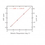
Fig. 1 Energy shift (as measured using the Bragg angle of a Si (18 12 6) reflection) versus the temperature of a (13 13 13) backscattering crystal. Solid line is a linear fit. Scan range was from 21.04 to 36.41 C.
The analyzer crystals are perhaps the single most difficult component of the IXS setup. They must be perfect (variations in lattice spacing, Δd/d, <~2×10⁻⁸) and must be spherically curved to accept a large solid angle. The required level of perfection means that it is not possible to simply bend a silicon wafer as the strain introduced by bending is too large. Thus we have adopted a method where many small perfect "crystallites" (each ~0.6×0.6×2.9 mm3) are attached to a well polished substrate of appropriate curvature (see Fig. 2), similar to [3]. One notable departure from the previous work, however, is the use of a high temperature metal diffusion bond to attach the crystallites to the substrate, instead of epoxy.
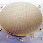
Fig. 2 Photograph of one analyzer crystal -10 cm diameter.
The important parameters for the analyzer crystal are the strain of the crystallites and their slope error. The strain was investigated in crystallites bonded to flat substrates [2] and it was shown that sufficient etching could make the response of a bonded crystallite the same as that of a flat perfect crystal. Notably, it was also shown that the etch could be applied either before or after the bond with nearly identical results. The slope error, or how exactly the orientation of the bonded crystal planes conforms to that of the substrate, has been investigated using an x-ray generator [4]: rocking curves of many single crystallites were measured and their center was compared with that expected for an ideal sample. Recently the 9.8m radii samples (intended for the highest resolution IXS measurements) show rms. deviations from the ideal shape of 20 to 30 μrad (Fig. 3). While reduction to the ~<10 μrad level is really desirable for sub-meV resolution, this is already rather good.

Fig. 3 Slope error for crystallites bonded to 9.8 radius spherical substrate. See text.
3. Instrumentation for Nuclear Resonant Scattering.
The late delivery of the spectrometer has provided some opportunity to work on nuclear resonant scattering. Where-as work with the 14.4 keV 57Fe resonance is relatively commonplace and can be done at several other beamlines at SPring-8 and throughout the world, we chose to begin work on a different isotope: the 25.65 keV resonance of 161Dy. The nuclear resonance in this transition metal has a relatively convenient (40 ns) lifetime, reasonable (19%) natural abundance and a large cross-section (low internal conversion) making it an excellent candidate for nuclear resonant scattering experiments using synchrotron radiation. The higher energy of the resonant transition also means that it is well suited to SPring-8, where the electron beam energy is high. However, significant, and largely original work is needed for the instrumentation, both for the high resolution monochromator and for the detector.
The optics design is challenging because the available high order reflections in silicon, either the (15 15 7) or the (18 12 6) are awkward to work with. The tiny, 0.13 μrad, angular acceptance of the (15 15 7) provides severe constraints on the crystal perfection, while the 87.4 degree Bragg angle of the (18 12 6) means the angular acceptance is bigger (0.48 μrad) but also makes conventional designs physically very large, and therefore susceptible to thermal drifts, crystal, imperfections, etc. Thus, building on the work of Ishikawa et al. [5] and Yabashi and Ishikawa [6], a new design [7] was made, as is shown in Fig. 4. Here a low order "coupling" crystal is used inside of the high order channel cut crystal. By allowing the beam to transmit through the coupling crystal, an extremely compact design is possible. This monochromator, used in the last cycles of 2000B, provided extremely good results, with a peak throughput of 2×10⁸ photons/second in a bandwidth of 0.52 meV. Use later (when the high heat load monochromator was performing less well) showed slightly reduced performance, with peak throughput of ~1.5×10⁸ and slightly (10-20%) larger bandwidth. Fig. 5. shows the spectrum of inelastic nuclear absorption from an enriched sample of Dy2O3. The good resolution of the peaks in the scattering, and the fast fall-off the tails of the monochromator response (essentially gone by ~2 meV from the peak) confirm its good response. In addition, the left and right-hand sides of the spectra (corresponding to phonon annihilation and creation, respectively) obey, exactly, detailed balance, confirming the quality of the data at a fairly high level.
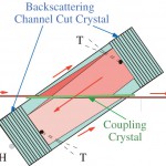
Fig. 4 New compact monochromator design for Bragg reflections near backscattering. Red arrows show beam direction, T and H indicate thermistors and a heater used for precise (~ 1mK) temperature measurement and control. See text.
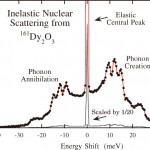
Fig. 5 Inelastic nuclear absorption from phonons in 161Dy2O3.
See text.
Nuclear forward scattering (NFS) with dysprosium provides a special challenge for detector development. Hyperfine splittings at the Dy nucleus may reach the level of 10 GHz, so that beat frequencies in the nuclear forward scattering can have periods ~ 100 ps. Therefore a detector with extremely good time resolution is desirable. However, due to the small bandwidth of the resonance (~16 neV), signal rates are generally low, so an efficient detector is also required. This poses severe problems for the use of standard silicon APDs at normal incidence, where a thicker (more efficient) device results in a poorer time resolution (this is due to the saturation of the electron drift velocity in silicon). Thus the x-ray detector with the best available (~100 ps) resolution [8] would have an efficiency of only ~0.5% at 25.6 keV. In order to combat this problem, we performed first tests of an array device in a grazing incidence geometry (see Fig. 6a). Using sixteen channels (each 1×2.5 mm2) on a 1.1 mm pitch, we have succeeded in generating a device having ~20% efficiency at 25.6 keV over a spot size of 0.75×2.5 mm2 [9]. The individual elements have a time resolution of ~160 ps while, for all channels, operating together, the resolution was ~200 ps. The time response for nuclear forward scattering from a Dy foil is shown in Fig. 6b and demonstrates the performance of the detector.
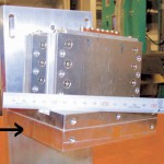
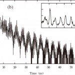
Fig. 6 (a) Photo of the 16 channel array detector (and amplifiers). Arrow shows window and approximate beam direction. (b) Nuclear forward scattering from a Dy foil measured with this detector. The inset shows a 5 ns range on a linear scale.
4. Summary.
The commissioning of BL35XU has begun in earnest, with instrumentation development for both IXS and NRS. With the recent (near) completion of the spectrometer mechanics, commissioning of the IXS setup will begin during in 2001A, on a base of instrumentation that has been tested and developed both on and off line. While all eventualities can not be anticipated, it is expected that the beamline will be open for user proposals in the fall of 2001. The user community is urged to contact beamline personnel to discuss experiments before (or concurrently with) proposal submission.
5. Acknowledgements.
The authors are grateful to the SPring-8 technical and administrative staff for making this project possible. Thanks are due especially to K. Takeshita, S. Goto and T. Matsushita for work on the beamline construction and design. In addition, the authors are grateful to A.I. Chumakov and M. Yabashi for collaboration on various commissioning work, T. Ohata and Y. Furukawa for help with control software, M. Sato for help during part of the commissioning, and T. Oguchi, Y. Kusaka, N. Inoue for technical support.
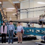
Beamline personnel in front of the new inelastic scattering spectrometer. The 3m vertical arm is visible at the upper left while the first part of the 10m arm is visible to the right. Form left to right: A. Baron, D. Miwa, D. Ishikawa, and Y. Tanaka.
6. References.
[1] A. Q. R. Baron, Y. Tanaka, S. Goto, K. Takeshita, T. Matsushita, and T. Ishikawa : J. Phys. Chem. of Solids 61 (2000) 461.
[2] A. Q. R. Baron, Y. Tanaka, D. Miwa, D. Ishikawa, T. Mochizuki, K. Takeshita, S. Goto, T. Matsushita, and T. Ishikawa : To Be Published in NIM A (2001)
[3] C. Masciovecchio, U. Bergmann, M. Kirsch, G. Ruocco, F. Sette, and R. Verbeni : Nucl. Instrumen. and Meth. B 111 (1996) 181 and B 117 (1996) 339.
[4] D. Miwa, A. Q. R. Baron, Y. Tanaka, D. Ishikawa, T. Ishikawa, H. Kimura, and F. Yamamoto : Unpublished.
[5] T. Ishikawa, Y. Yoda, K. Izumi, C. K. Suzuki, X. W. Zhang, M. Ando, and S. Kikuta : Rev. Sci. Instrumen. 63 (1992) 1015.
[6] M. Yabashi and T. Ishikawa : SPring-8 Annual Report (1999) 151.
[7] A. Q. R. Baron, Y. Tanaka, D. Ishikawa, D. Miwa, M. Yabashi, and T. Ishikawa : Submitted for Publication.
[8] S. Kishimoto : Nucl. Instrumen. and Meth. A 351 (1994) 554.
[9] A. Baron, M. Yabashi, T. Kudo and T. Ishikawa, et al. : to be published.
Alfred Q.R. Baron
Japan Synchrotron Radiation Research Institute(JASRI)
((財)高輝度光科学研究センター)
1-1-1, Kouto, Mikazuki, Sayo, Hyogo 679-5198, JAPAN
(〒679-5198 兵庫県佐用郡三日月町光都1-1-1)
TEL・FAX:0791-58-1816
e-mail:baron@spring8.or.jp
Yoshikazu Tanaka(田中 良和)
The Institute of Physical and Chemical Research (RIKEN)
(理化学研究所)
1-1-1, Kouto, Mikazuki, Sayo, Hyogo 679-5148, JAPAN
(〒679-5148 兵庫県佐用郡三日月町光都1-1-1)
TEL:0791-58-2931 FAX:0791-58-2923
e-mail:ytanaka@postman.riken.go.jp
Tetsuya Ishikawa(石川 哲也)
The Institute of Physical and Chemical Research (RIKEN)
(理化学研究所)
1-1-1, Kouto, Mikazuki, Sayo, Hyogo 679-5148, JAPAN
(〒679-5148 兵庫県佐用郡三日月町光都1-1-1)
TEL:0791-58-2805 FAX:0791-58-2807
e-mail:ishikawa@spring8.or.jp
