Volume 15, No.1 Pages 14 - 19
2. ビームライン/BEAMLINES
Status of the RIKEN Quantum NanoDynamics Beamline (BL43LXU):
The Next Generation for Inelastic X-Ray Scattering.
Materials Dynamics Laboratory, RIKEN SPring-8 Center / Research & Utilization Division, JASRI
- Abstract
- BL43LXU, the RIKEN Quantum NanoDynamics Beamline will be a world-leading facility using non-resonant inelastic x-ray scattering (IXS) to investigate atomic and electronic dynamics by directly probing the A2 contribution to the dynamic structure factor, S(Q,ω). Resolutions from < 1 to ~100 meV will be available via two spectrometers: a high-resolution instrument with a 10 m arm; and a medium-resolution instrument with a 2 m arm. Here we describe the status and over-all design of the beamline, including the source, which is expected to provide unprecedented flux and brilliance between 14.4 and 26 keV. First light is expected before the end of 2011.
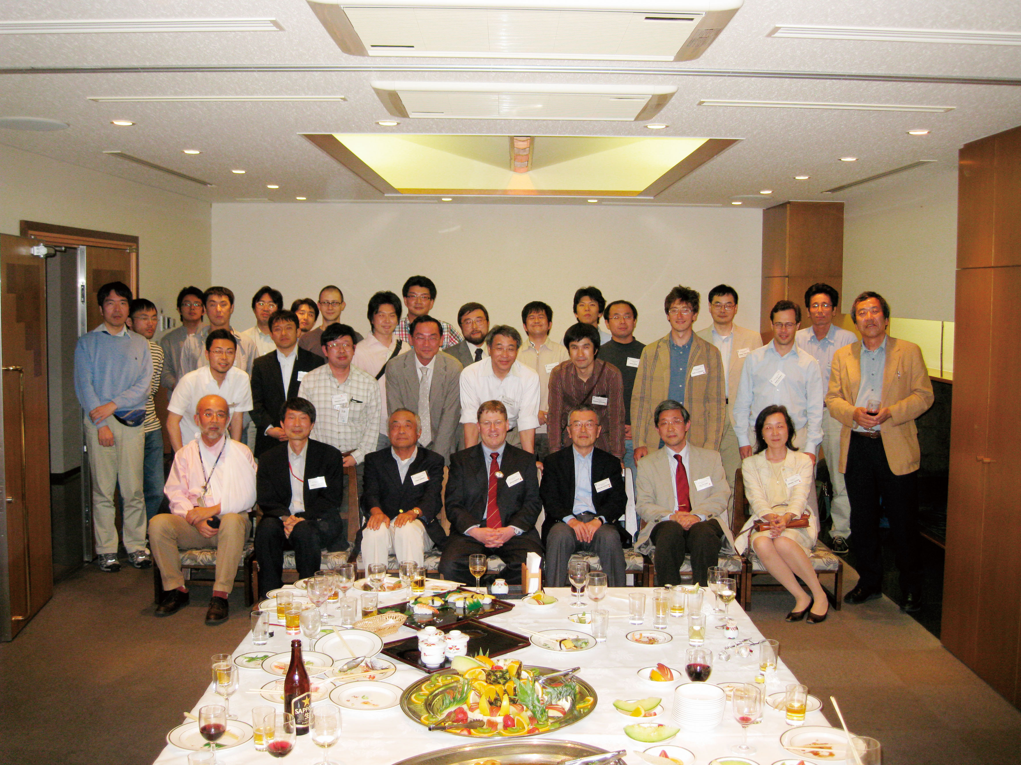
The RIKEN Quantum NanoDynamics Beamline, BL43LXU, will be a next generation facility for inelastic x-ray scattering (IXS). The purpose of the beamline is investigation of atomic and electronic dynamics with resolution from < 1 meV to ~100 meV, spanning momentum transfers from ~0.1 nm-1 to ~150 nm-1, and energy transfers from ~0.5 meV to > 10 eV, via non-resonant inelastic x-ray scattering. Of particular note is the use of a long insertion device to increase flux on the sample by about a factor of 10 over present instruments, a crucial improvement given the flux-limited nature of many IXS experiments. The beamline has been funded by MEXT through RIKEN with a 3-year maru-sai budget, beginning in FY2009. Several workshops have been held to discuss the scientific case for the beamline[1][1] Workshops included the “Workshop on High-Resolution IXS” in 2006, the “Workshop for a NanoDynamics Beamline:” in 2008, and a workshop on “Spectroscopy and Instrumentation for IXS” (SIIXS) in 2009. (Figure 1), and, even before those discussions, a team of scientists from SPring-8 had begun conceptual design work to address some of the associated technical hurdles[2][2] The team included A. Q. R. Baron, T. Mochizuki, H. Tanaka, K. Soutome, T. Takahashi, T. Tanaka, H. Ohashi and S. Goto, among others..

Figure 1 Photograph during the NanoDynamics Beamline workshop in 2008.
The present article describes the design and expected performance of BL43LXU. As this is a short report in a facility-based publication, the focus will be an overview of the expected capabilities of the beamline for those with some background in synchrotron radiation instrumentation. For a broader context as to how the instrument and the applications discussed here fit into the over-all picture of solid-state physics and x-ray scattering, we refer the reader to, e.g., the recent overview issue of Kotai Butsuri[3][3] 固体物理 44, For IXS in particular, see A.Q.R. Baron, 固体物理 44 (2009) 727-742. (Solid State Physics (Kotai Butsuri) 44 (2009) 727-742).. One crucial issue, though, is that while IXS experiments provide superior quality data, with nearly no background (see discussion in[4][4] A. Q. R. Baron : 分光研究第58巻第5号 (2009) pp.205-214 (Journal of The Spectroscopical Society of Japan Vol.58 #5 (2009) 205-214 (Japanese) or arXiv 0910.5764 (English)).), they remain severely count-rate limited. This is true for measurements of atomic dynamics in complex materials, or with complex sample environments, where scan times can be days. It is even more of an issue for measurements of electronic dynamics, where the cross sections are reduced. Thus, the improved source strength is a very important aspect of the beamline. Also of note is that BL43LXU will do non-resonant high-resolution investigation of electronic excitations at larger momentum transfer, which might be considered the momentum-resolved extension of optical or IR or Raman spectroscopy. This new field will allow access to both correlations in low-energy transitions (such as orbitons) and access to the higher order multipole character of localized transitions.
At the time of the writing of this article, January of 2010, most of the specifications for equipment for BL43LXU have been fixed, and the main components are now out for bid, with contracts to be set before April of 2010. Thus, the over-all design of the beamline is well established. First light is expected late in 2011, and first experiments in 2012. One should note that the present paper discusses the expected performance when the beamline is fully operational - achieving these goals will encompass the first few years of beamline operation.
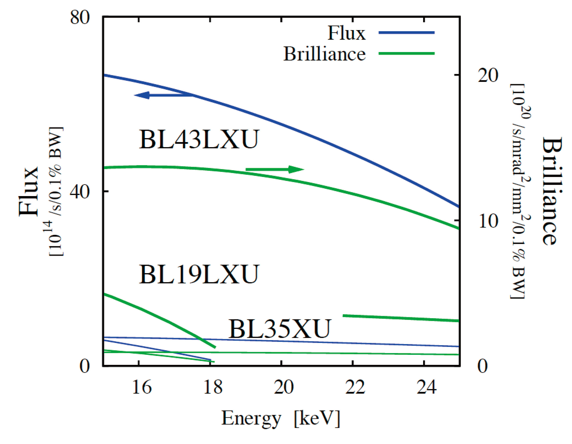
BL43LXU will take advantage of the strengths of the SPring-8 storage ring, including the high, 8 GeV, electron beam energy, the availability of a long (30 m) straight section, and in-vacuum undulator technology to produce a uniquely powerful source in the hard x-ray region. Specifically, the use of a three 5 m insertion devices (IDs) in series, each with a 19 mm period and a 6 mm minimum magnetic gap, will allow unprecedented flux and brilliance between 14.4 and 26 keV (kmax = 1.56 at 14.4 keV, k~1 at 22 keV). Calculated flux and brilliance is shown in Figure 2. Importantly, the short undulator period and 8 GeV electron energy of the storage ring allows this range of x-ray energy to be covered in the fundamental of the undulator, leading to a favorable ratio of useful flux to heat load. However, to achieve the small gap for this requires intermediate focusing of the electron beam, with magnets (quadrupoles and sextupoles) between the undulator segments, to keep the electron beam size small enough for the 6 mm gap, and to retain sufficient injection aperture[6][6] K. Soutome, Y. Shimosaki, J. Schimizu, M. Takao, M. Oishi, M. Shoji, Y. Okayasu, K. Fukami, C. Mitsuda and H. Yonehara : unpublished.. While this reduces the length of the insertion device to 15 m (as compared, say, to the 24 m ID at BL19LXU) there is still a large gain in both brilliance and flux over the desired energy range (see Figure 2). For those who may wonder about the performance of this beamline as compared to the SPring-8 x-ray free electron laser (XFEL), we note that the XFEL is a pulsed source and, while the peak pulse intensity is very large, the time-averaged flux per unit bandwidth (which is the relevant figure of merit for IXS) of the XFEL will be much (~103 times) less than at BL43LXU.

Figure 2 Flux and Brilliance
Calculated flux and brilliance for a standard SPring-8 insertion device (ID), 4.5 m long, 32 mm period, as at BL35XU, the 24 m ID at BL19LXU (also 32 mm period), and the 15 m, 19 mm period, ID planned for BL43LXU. Calculations using SPECTRA[5][5] T. Tanaka and H. Kitamura : Journal of Synchrotron Radiation 8 (2001) 1221 and http://radiant.harima. riken.go.jp/spectra/index.html.. Flux calculations have assumed a fixed front-end slit size for each ID. For BL19LXU, only the Brilliance is shown, and the gap in the tuning curve is due to the large (12 mm) minimum aperture at BL19LXU, which has no intermediate electron-beam focusing. For BL43LXU, the calculations have been done assuming a single undulator of 15 m length.
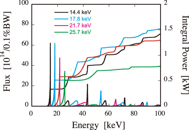
The power load on the pink-beam components is a serious concern. While operation of the insertion device in the fundamental improves the flux to power load ratio, the long insertion device still has a large total power, ~47 kW at minimum gap, and an extremely high peak power (about 3 MW/mrad2) based on calculations using SPECTRA[5][5] T. Tanaka and H. Kitamura : Journal of Synchrotron Radiation 8 (2001) 1221 and http://radiant.harima. riken.go.jp/spectra/index.html.. With some re-design, and thanks to the good thermal properties of glidcop, the front-end is expected to survive these power loads[7][7] S. Takahashi, Private Communication and S. Takahashi, M. Sano, T. Mochizuki, A. Watanabe and H. Kitamura : Journal of Synchrotron Radiation 15 (2008) 144.. However the power onto the monochromator remains a serious problem, with the central cone expected to be ~1.8 kW at minimum gap. Liquid nitrogen cooling of a silicon monochromator crystal has been shown to be effective up to ~700 W[8][8] A. I. Chumakov : Private Communication., but the expected power at BL43LXU is more than double that, with a substantially higher power density. BL43LXU will therefore use a liquid nitrogen cooled mirror upstream of the monochromator (M1 in Figure 4) to reduce the power onto the monochromator by removing the x-rays form the higher undulator harmonics (see Figure 3). Cooling the silicon using liquid nitrogen to a temperature near to the zero in the thermal expansion, and the large beam footprint, should reduce the thermal distortion of the mirror from ~1 kW absorbed power to ~0.4 microradians[9][9] Based on finite element (ANSYS) calculations by T. Mochizuki.. It is hoped to reduce this even to the 0.1 microradian level by gently bending the mirror. A diamond monochromator was also considered, but difficulties in removing the expected power deposition (~100 W, even for a thin diamond) and issues of crystal quality and performance (especially at higher energy) led to a preference for the nitrogen cooled silicon mirror. A matched mirror (M2 in Figure 4) will be installed after the mono to return the beam to horizontal. It is worth noting that mirror technology has progressed to a point where substantially sub-microradian slope errors are possible on long flat mirrors (the mirrors are specified to have < 0.3 micro-radian tangential slope error over the central 800 x 60 mm2).

Figure 3 Calculated spectra and integrated power for several settings of the BL43LXU undulator.
The front-end slit size has been chosen to keep the power absorbed by the first mirror < 1 kW and the power absorbed by the mono < 550 W. The power is the flux integrated from low energy to the value given on the x-axis. The mirror will act to cut-off that part of the power at energies above the fundamental, so at the first plateau of the power curve.

Figure 4 Planned hutch layout for BL43LXU.
Beam from the undulator is incident from the left, and for the high resolution spectrometer, is backscattered by the BX mono (far right), and impinges on the sample from the right. M1 is the nitrogen cooled mirror, M2 the matched mirror to return the beam to horizontal and M3 the focusing cylindrical mirror for the high resolution scattering. The length of the displayed hutches is 47 m.
The beamline will have two main instruments, as shown in the layout presented in Figure 4: a large high-resolution spectrometer and a smaller medium-resolution spectrometer. The high-resolution spectrometer will be for measurements with good momentum resolution, a small fraction of a Brillouin zone (typical analyzer acceptance between ~1 x 5 and 10 x 10 mrad2, or momentum resolution in one dimension between about ~0.1 and 1 nm-1), and energy resolution between < 1 and 40 meV (see also Table 1). The better energy resolution will be used for measuring atomic dynamics, with the relaxed resolution (6 and 40 meV) to permit higher rates for lower cross-section experiments, especially those investigating electronic excitations. The medium resolution instrument will be primarily for electronic excitations, and will have larger acceptance (~50 x 50 mrad2) analyzers on a short, ~2 m, arm. It will operate primarily at 15.816 keV (corresponding to the Si(888) back reflection for the analyzer crystals) and is expected to have energy resolution between 10 and 100 meV, depending on the choice of incident beam monochromatization. Both spectrometers will operate with a horizontal scattering plane. The high-resolution spectrometer will have a maximum scattering angle of ~55 degrees, while the medium resolution spectrometer will scan to ~130 degrees in two-theta. For scattering angles near to 90 degrees on the medium resolution spectrometer, a diamond half-wave plate will be employed to rotate the plane of the polarization to vertical and to reduce losses from pi-polarized Thomson scattering. We note that early designs considered a single spectrometer with an arm length of about 6 m. However, this was finally discarded, as being less than optimal for many experiments: the 6 m arm length, as compared to the 10 m now planned, would make sub-meV work difficult, while for medium resolution a shorter, ~2 m, arm was desirable to increase analyzer solid angle and therefore count rates.
Table 1 Expected operating conditions for BL43LXU.
| Resolution (meV) |
X-Ray Energy (keV) |
ΔQmax (nm-1) |
Emax (eV) |
Qmax (Å-1) |
Analyzer | Source Flux (GHz/meV) |
| < 0.9 | 25.7 | 1.2 | 4.9 | 12 | Si(13 13 13) | 140 |
| 1.4 | 21.7 | 1.0 | 4.1 | 10 | Si(11 11 11) | 230 |
| 2.8 | 17.8 | 0.8 | 3.4 | 8.3 | Si(9 9 9) | 390 |
| 6.0 | 15.8 | 0.7 | 3.0 | 7.4 | Si(8 8 8) | 440 |
| 40 | 15.8 | 0.7 | 10 | 7.4 | Si(8 8 8) | 440 |
| 10-100 | 15.8 | 3.4 | > 10 | 16 | Si(8 8 8) | 440 |
| > 0.3 | 14.4 | > 0.3 | > 10 | 15 | 57Fe Nuclear | 430 |
All operating conditions, except the last two lines, refer to the large high-resolution spectrometer with a 10 m two-theta arm. Qmax and Emax are the maximum momentum and energy transfers accessible. ΔQmax is the maximum acceptance for a single analyzer - the lower limit will be < 0.1 nm-1 (limited by count-rate) for the high-resolution spectrometer. The last two lines are for the medium resolution spectrometer for electronic excitations, and the nuclear resonant scattering (NRS) setup, respectively. The resolution, in energy and momentum, for the NRS setup, will be primarily count-rate limited, with the values listed based on an estimate for a sample with relatively high rate (light elements).
It is worth taking a moment to comment on the planned operating energy range, and modes of operation. The energy range is largely dictated by using silicon optics in a near-backscattering geometry: silicon remains the material of choice when large-area highly-perfect crystals are needed, while the backscattering geometry (Bragg angles near to 90 degrees) is desirable to get maximum angular acceptance for a given energy resolution, as can be seen by differentiating Bragg's law. However, silicon backscattering optics quickly become inefficient at higher energy, with reflectivity dropping fast as x-ray energies approach 30 keV. Meanwhile, from the point of view of sample investigation, higher energy, for a fixed incident flux (in units of photons/s/meV), is almost always better, as this allows one to get higher rates from larger samples due to reduced photoelectric absorption, and also to more easily penetrate into complex sample environments. Thus, the 15-26 keV energy range, which covers intrinsic resolutions in backscattering from about 4 to 0.3 meV (single reflection bandwidth in silicon) is a very reasonable one. Finally, the extension of the operating energy range down to 14.4 keV is to match the nuclear resonance in 57Fe. This resonance has an intrinsic linewidth of < 10 µeV, so, in principle, using time-gating and a nuclear analyzer, as discussed in[10][10] A. I. Chumakov, A. Q. R. Baron, R. Ruffer, H. Grunsteudel, H. F. Grunsteudel and A. Meyer : Phys. Rev. Lett. 76 (1996) 4258., very high resolution experiments will be possible (estimates suggest 0.3 meV resolution should be possible). Table 1 summarizes the expected operating conditions.
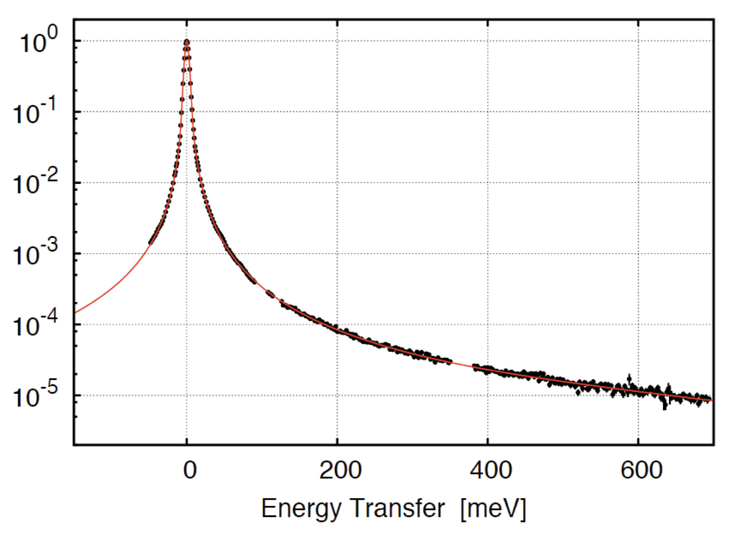
The medium resolution spectrometer will use analyzers operating at the silicon (888) back-reflection with a temperature gradient[11][11] D. Ishikawa and A. Q. R. Baron : Journal of Synchrotron Radiation 17 (2010) 12-24. to allow large space at the sample with a resolution of ~10 meV. This resolution can then be relaxed to gain flux by increasing the incident bandwidth. It is worth emphasizing that one of the reasons to use the (888) analyzer reflection instead of the (555) as is sometimes done, is the relatively good response of the tails. The tails of Bragg reflections increase as the square of their width−if ΔED is the intrinsic (energy) Darwin width of the reflection (nearly the full width at half maximum) centered at E0 the reflectivity at an energy E with |E-E0| >> ΔED is just R ≈ (ΔED)2 / (4(E-E0))2. Relaxing the resolution, increasing ΔED, of the analyzer in an effort to get more counts, results in tails increasing as the square of the width, which is a very serious concern for measurements at smaller energy transfers. Figure 5 shows the resolution function from a setup where a single-reflection Si(888) monochromator is used with a Si(888) analyzer, which has been used to measure a d-d excitation in NiO[12][12] A. Q. R. Baron et al.: Unpublished.. The integral intensity of the d-d excitation was some 3 orders of magnitude less than phonon intensity, and the peak some 4 orders of magnitude reduced. Thus the tails are very important. Comparing the Si(888) with its 4 meV Darwin width, against the Si(555) which has a 14 meV width at 10 keV, one can expect measure excitations about a factor of 2 to 3 closer to phonon lines using the Si (888) analyzer.

Figure 5 Resolution function using the silicon (888) reflection. (4 meV Darwin width for the analyzer and the monochromator). Note points removed near 100 and 350 meV correspond to known excitation bands in the plexi-glass sample used to simulate inelastic an elastic response. The solid line is a smooth curve fit to the data.
We briefly mention some of the expected improvements, in addition to higher flux, beyond the instrument BL35XU. The first is that the analyzer array on the 10 m arm will be increased in size, with a planned goal of 42 elements (as opposed to the 12 at BL35XU). As the data rate, for some experiments, scales linearly with the number of analyzers, this is a large improvement. In addition, these analyzers will take advantage of a new design concept so that when a temperature gradient is applied to them[11][11] D. Ishikawa and A. Q. R. Baron : Journal of Synchrotron Radiation 17 (2010) 12-24., combined with an efficient position sensitive detector (such a detector is being developed now[13][13] H. Toyokawa, Y. Furukawa, T. Hirono, H. Ikeda, K. Kajiwara, M. Kawase, T. Ohata, G. Sato, M. Sato, T. Takahashi, H. Tanida, T. Uruga and S. Watanabe : To Be Published in the Proceedings of the Hiroshima Symposium On The Development And Application Of Semiconductor Tracking Detectors.), improved resolution may be possible. The long-term goal is ~0.7 meV at 25.7 keV and 1.3 meV resolution at 21.7 keV (FWHM). The default beam size at BL43LXU is expected to be smaller, compared to that at BL35XU due to improvements in mirror technology and placement. In particular, the bent cylindrical mirror (M3) is expected to focus the beam to about 20 x 35 µm2 in the full width at half maximum, including the effects of mirror slope error. This is good for focusing an entire beam at ~20 keV without losses, and will allow most experiments to be performed. Focusing to smaller size, ~5 microns or less, is expected, and is under consideration, though it will reduce the flux onto the sample.
The paper has introduced the RIKEN Quantum NanoDynamics beamline, BL43LXU, discussing the main capabilities and over-all design. Science at the beamline will (1) directly build on the studies of atomic dynamics at BL35XU, and (2) enter the new field of high-resolution measurement of electronic excitations. Directions of work in the first category include phonons in larger-unit-cell correlated materials where both good momentum and good energy resolution are required, extreme and geologically relevant environments (including high-pressure and high temperature conditions in diamond anvil cells), atomic dynamics associated with liquid phase transitions, and the detailed behavior of the atomic dynamics of glasses. All of these fields are now limited by count-rate at present instruments, and their extension, and the path to new and important data at BL43LXU, is relatively straightforward. In addition, the high-resolution measurements of electronic dynamics (with demonstration experiments recently done) will provide a window into new science, with one target being dispersion of low-energy electronic excitations such as orbitons, and another being the details of structure of electronic transitions, including extending investigations of features known from more conventional spectroscopic methods (IR, oprical, Raman) to higher momentum transfers.
Acknowledgements:
This project has had help from many of the scientists and administrative staff at SPring-8. The contributions of M. Abe, H. Aoyagi, H. Arita, K. Fukami, H. Fukui, Y. Furukawa, S. Goto, Y. Harada, D. Ishikawa, Y. Ishizawa, H. Kimura, H. Kitamura, H. Konishi, T. Matsushita, T. Mochizuki, H. Ohashi, T. Ohata, H. Ohkuma, M. Oishi, S. Sasaki, J. Shimizu, Y. Senba, M. Shoji, K. Sorimachi, K. Soutome, S. Takahashi, M. Takata, K. Takeshita, T. Takeuchi, H. Tanaka, T. Tanaka, S. Tsutsui, H. Uchiyama, J. Yahiro, H. Yamazaki, and the strong support of the RIKEN SPring-8 Center Director, T. Ishikawa, are gratefully acknowledged.
References
[1] Workshops included the “Workshop on High-Resolution IXS” in 2006, the “Workshop for a NanoDynamics Beamline:” in 2008, and a workshop on “Spectroscopy and Instrumentation for IXS” (SIIXS) in 2009.
[2] The team included A. Q. R. Baron, T. Mochizuki, H. Tanaka, K. Soutome, T. Takahashi, T. Tanaka, H. Ohashi and S. Goto, among others.
[3] 固体物理 44 For IXS in particular, see A.Q.R. Baron, 固体物理 44 (2009) 727-742. (Solid State Physics (Kotai Butsuri) 44 (2009) 727-742).
[4] A. Q. R. Baron : 分光研究第58巻第5号 (2009) pp.205-214 (Journal of The Spectroscopical Society of Japan Vol.58, #5 (2009) 205-214 (Japanese) or arXiv 0910.5764 (English)).
[5] T. Tanaka and H. Kitamura : Journal of Synchrotron Radiation 8 (2001) 1221 and http://radiant.harima. riken.go.jp/spectra/index.html.
[6] K. Soutome, Y. Shimosaki, J. Schimizu, M. Takao, M. Oishi, M. Shoji, Y. Okayasu, K. Fukami, C. Mitsuda and H. Yonehara : unpublished.
[7] S. Takahashi, Private Communication and S. Takahashi, M. Sano, T. Mochizuki, A. Watanabe and H. Kitamura : Journal of Synchrotron Radiation 15 (2008) 144.
[8] A. I. Chumakov : Private Communication.
[9] Based on finite element (ANSYS) calculations by T. Mochizuki.
[10] A. I. Chumakov, A. Q. R. Baron, R. Ruffer, H. Grunsteudel, H. F. Grunsteudel and A. Meyer : Phys. Rev. Lett. 76 (1996) 4258.
[11] D. Ishikawa and A. Q. R. Baron : Journal of Synchrotron Radiation 17 (2010) 12-24.
[12] A. Q. R. Baron et al.: Unpublished.
[13] H. Toyokawa, Y. Furukawa, T. Hirono, H. Ikeda, K. Kajiwara, M. Kawase, T. Ohata, G. Sato, M. Sato, T. Takahashi, H. Tanida, T. Uruga and S. Watanabe : To Be Published in the Proceedings of the Hiroshima Symposium On The Development And Application Of Semiconductor Tracking Detectors.
Alfred Q. R. Baron
Materials Dynamics Laboratory, RIKEN SPring-8 Center,
1-1-1 Kouto, Sayo, Hyogo, 679-5148
&
Research and Utilization Division, SPring-8/JASRI,
1-1-1, Kouto, Sayo, Hyogo 679-5198
TEL:0791-58-0803 x 3883 FAX:0791-58-1816
e-mail: baron@spring8.or.jp


