


Volume 21, No.1 Pages 5 - 9
1. 最近の研究から/FROM LATEST RESEARCH
Long-term Proposal Report
Development of Spin-HAXPES Technique for the Exploration of the Electronic Structure of Buried Layers and Interfaces
[1]Max-Planck-Institut für Chemische Physik fester Stoffe, [2]Research & Utilization Division, JASRI
- Abstract
- We report on the first prototype of the spin-resolved hard x-ray photoelectron spectroscopy detector. The detector is based on Spin-Polarized Low-Energy Electron Diffraction (SPLEED) using a W(100) single-crystal. The detector is connected to a large hemispherical electron spectrometer (VG Scienta R-4000). Photoelectrons with selected kinetic energy are collected by the electron spectrometer and deflected to the spin detector. Using a photon energy of 5.95 keV, the spin resolved valence band of buried Co2Mn1.24Fe0.16Si0.84 films was measured.
1. Introduction
The tunneling of spin-polarized electrons from ferromagnetic electrodes through insulating barriers has attracted enormous interest due to its applicability in magnetic tunnel junctions (MTJs) and spin injection into semiconductors. The performance of these spintronic devices depends on the degree of spin polarization of the flowing electrical current. Therefore, the spin-resolved probing of electronic structures in buried ferromagnetic layers and interfaces is of great importance.
Spin-resolved photoelectron spectroscopy (SR-PES) is a powerful method providing direct information on the spin-dependent electronic structure of materials. The method in general is based on scattering of the polarized photoelectron beam at a target material with large atomic number. Due to the large spin-orbit interaction, electrons with opposite spins have different scattering cross sections resulting in asymmetries in their scattered beam intensities[1-3][1] J. Kirschner, G. Hohler (Ed.): Polarized Electrons at Surfaces: Springer Tracts in Modern Physics 106 (Springer, Berlin, 1985) 155.
[2] J. Kirschner and R. Feder: Physical Review Letters 42 (1979) 1008.
[3] M. Getzlaff et al.: Review of Scientific Instruments 69 (1998) 3913.. Owing to a high surface sensitivity, conventional ultraviolet PES and soft-x-ray PES are suited for the study of thin adsorbate overlayers, surface states and topologically protected edge states. However, the study of bulk properties and spintronic multilayer systems are not possible. The situation is different in the hard x-ray range. In hard x-ray photoelectron spectroscopy (HAXPES), true bulk information is provided, ruling out critical surface artifacts. The inelastic mean free path increases to typical values exceeding 10 nm. Hence, many atomic layers contribute to the total signal. A spin-resolved HAXPES measurement could directly and unambiguously probe the degree of spin polarization of multilayer structures and interfaces, providing an immense contribution to the spintronic industry.
In the present paper, we report on the development of the first prototype of spin-resolved HAXPES, the SPLEED-HAXPES. The buried MgO/Co2Mn1.24Fe0.16Si0.8 interface was probed using photon energy of 5.95 keV. The experiments were carried out in the beamlines BL09XU and BL47XU. We employed the SPLEED using W(100) target crystal as a spin detecter. Combining with Scienta R-4000 analyzer, the spin polarization of photoelectrons from the valence band states of the semi-metal could be measured. The spectra are compared with the theoretical spin-resolved density of states (DOS), which is calculated by fully relativistic SPR-KKR (spin-polarized relativistic Korringa-Kohn-Rostoker) Green's function method[4][4] H. Ebert, D. Ködderitzsch and J. Minar: Reports on Progress Physics 74 (2011) 096501., using the generalized gradient approximation (GGA), in a form proposed by Perdew, Burke and Ernzerhof (PBE) [5][5] J. P. Perdew, K. Burke and M. Ernzerhof: Physical Review Letters 77 (1996) 3865..
2. Experimental Details
Figure 1(a) shows the schematic layout of the setup. Photoelectrons with selected kinetic energy are collected by the electron analyzer and are deflected to the SPLEED detector entrance for spin detection. The SPLEED analyzer comprises a set of high voltage lens system, a W(100) target crystal and 4 channeltron electron multipliers. The SPLEED lens system collimates and decelerates the photoelectrons to a kinetic energy of 103 eV, which corresponds to the optimum energy for spin detection. The collimated photoelectron beam impinges on the W(100) crystal and the quasi-elastic scattered electrons are measured by the four channeltrons positioned symmetrically along the horizontal (2,0),(2,0) and vertical (0,2),(0,2) LEED directions (see Figure 1(b)). Implementation of spin-resolved HAXPES is unavoidably related to significant losses in signal intensity (at the spin discriminating system and reduced cross sections of high-energy photons[6][6] G. H. Fecher et al.: Journal of Physics. D: Applied Physics 40 (2007) 1576.). This poses particular limitations and requirements on this approach and requires additional instrumental development.
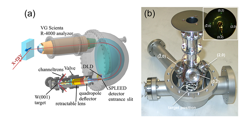
Figure 1. (a) Schematic layout of the spin-resolved HAXPES experimental setup, employing VG Scienta high-energy analyzer and SPLEED detector based on W(100). The blue arrow indicates magnetization direction. The other set of the measurement for opposite magnetization direction is also measured.
(b) Disassembled part of the SPLEED detector showing three of the four channeltrons, which are labeled according to the LEED scattering directions of the W(100) as shown in the inset of the figure.
The deceleration of the high-energy photoelectrons to the scattering energy of 103 eV is achieved in two steps: Firstly, the Scienta analyzer decelerates the electrons of the selected kinetic energy to the working pass energy (PE) of 200 eV. The photoelectrons are then further decelerated by the lens system of the SPLEED detector. During the scanning of the kinetic energies, the voltages in the SPLEED lens follow dynamically the retardation potential of the Herzog electrodes. Because the potential is relatively high (close to the photon energy), there is difficulty to prevent discharge problem. To avoid electric leakages and related problems, we decided to use independent systems for supplying power as shown in Figure 2. The voltage values of the lens system of the SPLEED detector and the Scienta analyzer are then interconnected through software.
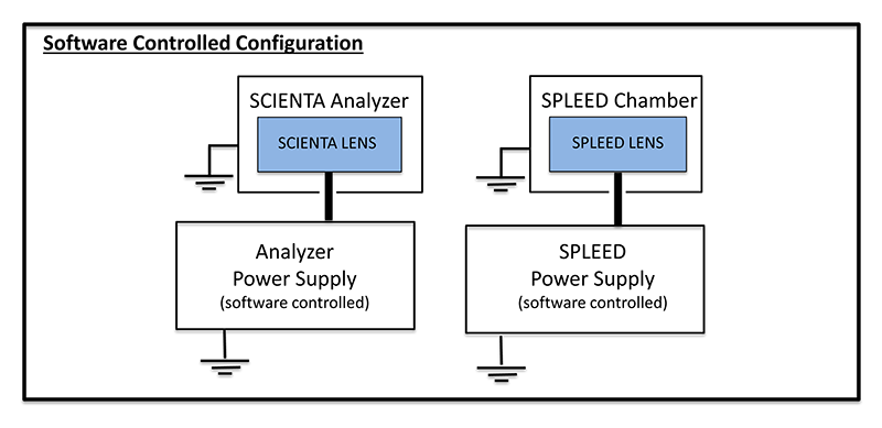
Figure 2. Power supply configuration. The two electrically independent high-voltage power supplies are digitally interconnected by software.
The front stage of the detector provides the maximal beam transmission, and the rear one with its Einzel lens facilitates the final focusing correction close to the target surface. Off-axial beam divergence correction is performed at the front stage by a set of quadrupole detector optics. Extensive simulations of electron trajectories were performed, by means of the SimIon software[7][7] SimIon Ion and Electron Optics Simulator [Computer Software] http://simion.com, in order to optimize the transmission of the transfer optics.
In the experiment, a photon energy of 5.95 keV was used. The beam with bandwidth of 50 meV, which delivers nearly 1012 photons/s photon flux at the focus position, is obtained by the primary Si(111) double crystal monochromator and the following downstream Si channel-cut monochromator where the (333) reflection plane is used[8][8] I. Galanakis et al.: Applied Physics Letters 89 (2006) 042502.. The beam, initially focused by a standard vertical mirror setup, is focused down to 12.4(H) × 4.6(V) μm2 by a pair of Kirkpatrick-Baez mirrors. The experiment was performed in normal emission geometry; a take-off angle of 88° was used. The total energy resolution (analyzer and spin-detector) of 760 meV was verified by Fermi cut-off measurements of an amorphous Au sample at room temperature.
A pair of identical samples with opposite horizontally oriented magnetization was mounted onto a sample holder. The measurements were performed with p-polarized light and the sample magnetization orientation parallel and antiparallel to the beam propagation. The spin asymmetry is expected to be measured along the vertical channeltrons; which are for counting photoelectron numbers I(0,2) and I(0,2). To exclude the instrumental asymmetry in the spin-resolved photoemission experiment, spectra were taken from both samples. Assigning IM+(-) to the signal intensity obtained from the samples with right (left) magnetization, the spin polarization, P, was derived as:
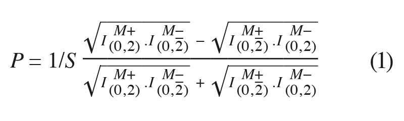
where S is the effective Sherman function equal to 0.25 for this detector. The experiment consists of measuring the spin polarization of the photoelectrons originating from the valence band of the half-metal. The asymmetry in intensities of the elastic scatterings measured by channeltrons mounted in opposite directions gives the degree of spin polarization. The spin-splitting efficiency of the W crystal is strongly suppressed by impurities adsorbed on the surface. For this reason, the crystal must be periodically cleaned by a flash annealing (1500 K for few seconds). The surface remains clean for approximately 40 minutes. The typical measurement cycle is illustrated in Figure 3. A entire cycle takes from 90 to 110 minutes.
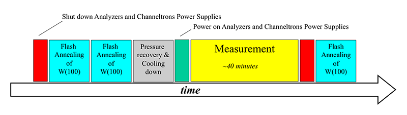
Figure 3. Measurement cycle. Each measurement is intercalated by two or more flash-annealings of the W(100) crystal.
3. Results and Discussion
The investigated multilayer structure with the film sequence: MgO(001) substrate/MgO buffer[10]/Co50Fe50 buffer[10]/Ir22Mn78[10]/Co50Fe50[1.1]/Co2Mn1.24Fe0.16Si0.90[20]/MgO[2]/AlOx[1] were grown using ultrahigh-vacuum magnetron sputtering deposition (numbers in brackets indicate the thickness in nm). According to calculations[8][8] I. Galanakis et al.: Applied Physics Letters 89 (2006) 042502. on Co2Mn1-xFexSi, it is possible to tune the Fermi edge EF position to the exactly the middle of the half-metal gap by change the Fe composition. This would maximize the spin polarization resulting in high Tunnel Magneto Resistance (TMR) ratios in magnetic tunneling junctions (MTJs) devices at EF. Experimental MTJs with the special composition, Co2Mn1.24Fe0.16Si0.84, were found to exhibit giant TMR ratios of 2610% at 4.2 K and 429% at 290 K. Therefore it is interesting to measure the spin polarization of the interface between the films with this composition and MgO.
The valence band photoemission spectra were measured for several days; the accumulated spectra for the upper and lower channeltrons are shown in the Figure 4(a) and (b), for two identical samples magnetized in-plane to the right (M+) and left (M-) orientation. The spin polarization, according to the equation (1), is shown in Figure 4(c). Despite the low statistics it is possible to observe an oscillatory behavior along the spectral energy. This is in agreement with calculations on spin polarization spectra expected for similar composition, Co2MnFe0.16Si0.84, as shown in the Figure 5. The calculation indicates a spin polarization of 100% at Fermi energy, while experimentally we obtained about 20%. It is not possible to state if the actual spin polarization is reduced at the MgO interface because intermixing or chemical disordering; or the difference of the spin polarization is due to an experimental error caused by the low statistics: the count rate at Fermi energy is inferior 1 count/sec.
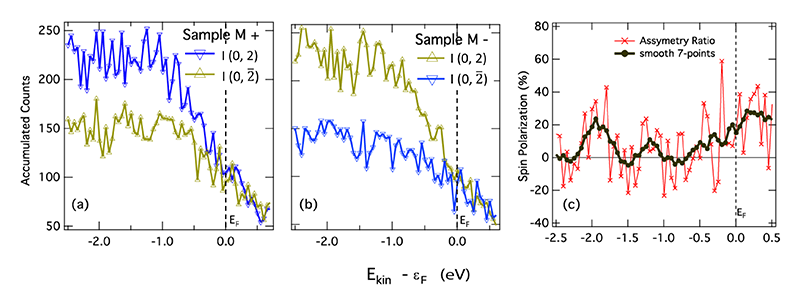
Figure 4. (a) and (b) Spin-resolved HAXPES measurements near EF.
(c) Spin polarization derived from the spectra in (a) and (b).
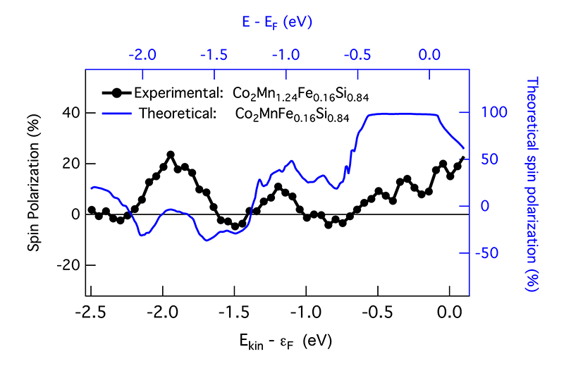
Figure 5. Comparison between spin polarizations derived from the asymmetry measured at the SPLEED detector and from ab-initio calculations. The ab-initio calculations were performed on Co2MnFe0.16Si0.84.
In summary, the experimental conditions were optimized to use a conventional spin detector based on SPLEED using a W(100) surface in HAXPES. We succeeded in measuring the spin resolving HAXPES spectra from buried interfaces, including the valence band. This result was achieved owing to significant improvements in the electronics, equipment and operating conditions of the SPLEED spin detector, as detailed above. The know-how obtained in this project is important for the construction of more advanced spin detectors working with high-energy, as for instance the 2D-multichannel detectors. Future analyzers derived from this prototype will play a crucial role in the research of spintronic materials.
Acknowledgements
Financial support by Deutsche Forschungsgemeinschaft and the Strategic International Cooperative Program of JST (DFG-JST) (Project P1.3-A of research unit FOR 1464: ASPIMATT) and by ERC 291472 IDEA Heusler are gratefully acknowledged. HAXPES experiments were performed at BL09XU and BL47XU of SPring-8 with approval of JASRI (Proposal No. 2012A0043-2014B0043: Long-term Proposal, and No. 2015A1614: General Proposal).
References
[1] J. Kirschner, G. Hohler (Ed.): Polarized Electrons at Surfaces: Springer Tracts in Modern Physics 106 (Springer, Berlin, 1985) 155.
[2] J. Kirschner and R. Feder: Physical Review Letters 42 (1979) 1008.
[3] M. Getzlaff et al.: Review of Scientific Instruments 69 (1998) 3913.
[4] H. Ebert, D. Ködderitzsch and J. Minar: Reports on Progress Physics 74 (2011) 096501.
[5] J. P. Perdew, K. Burke and M. Ernzerhof: Physical Review Letters 77 (1996) 3865.
[6] G. H. Fecher et al.: Journal of Physics. D: Applied Physics 40 (2007) 1576.
[7] SimIon Ion and Electron Optics Simulator [Computer Software] http://simion.com
[8] I. Galanakis et al.: Applied Physics Letters 89 (2006) 042502.