Volume 14, No.2 Pages 159 - 166
2. 最近の研究から/FROM LATEST RESEARCH
Long-term Proposal Report 4:
SUB-NANOSECOND STRUCTURAL SNAPSHOTS OF THE OPTICAL RECORDING PROCESS
[1]Center for Applied Near-Field Optics Research, National Institute of Advanced Industrial Science & Technology, [2]Japan Synchrotron Radiation Institute, SPring-8
1. Introduction
With the proliferation of electronic devices, the need for non-volatile, archival storage is ever increasing. The use of optical information encoding has proven to be a stalwart of long-term storage and is most often encountered in the form of the DVD standard. In the rewriteable form of the DVD, here exemplified by DVD-RAM media, information is stored as amorphous marks on a crystalline background. For the case of DVD-RAM, the recording layer is based upon an alloy of Ge, Sb, and Te, specifically the Ge2Sb2Te5 composition. Ge2Sb2Te5 is an indirect semiconductor with an optical bandgap of approximately 〜0.5 eV. The properties of these materials are unusual from several perspectives. First, the differences in electronic and physical properties of the amorphous and crystalline phases of Ge2Sb2Te5 are atypically large when compared to other semiconducting compounds such as Si or GaAs. In typical semiconductors, the creation of an amorphous phase typically results in the broadening of sharp features in the density of states and band tailing in the forbidden gap leading to small changes in minor changes in electronic effects such as the complex index of refraction and a smaller bandgap, respectively. In addition, the asymmetry of the interatomic potential often leads to an increase in bonding lengths.
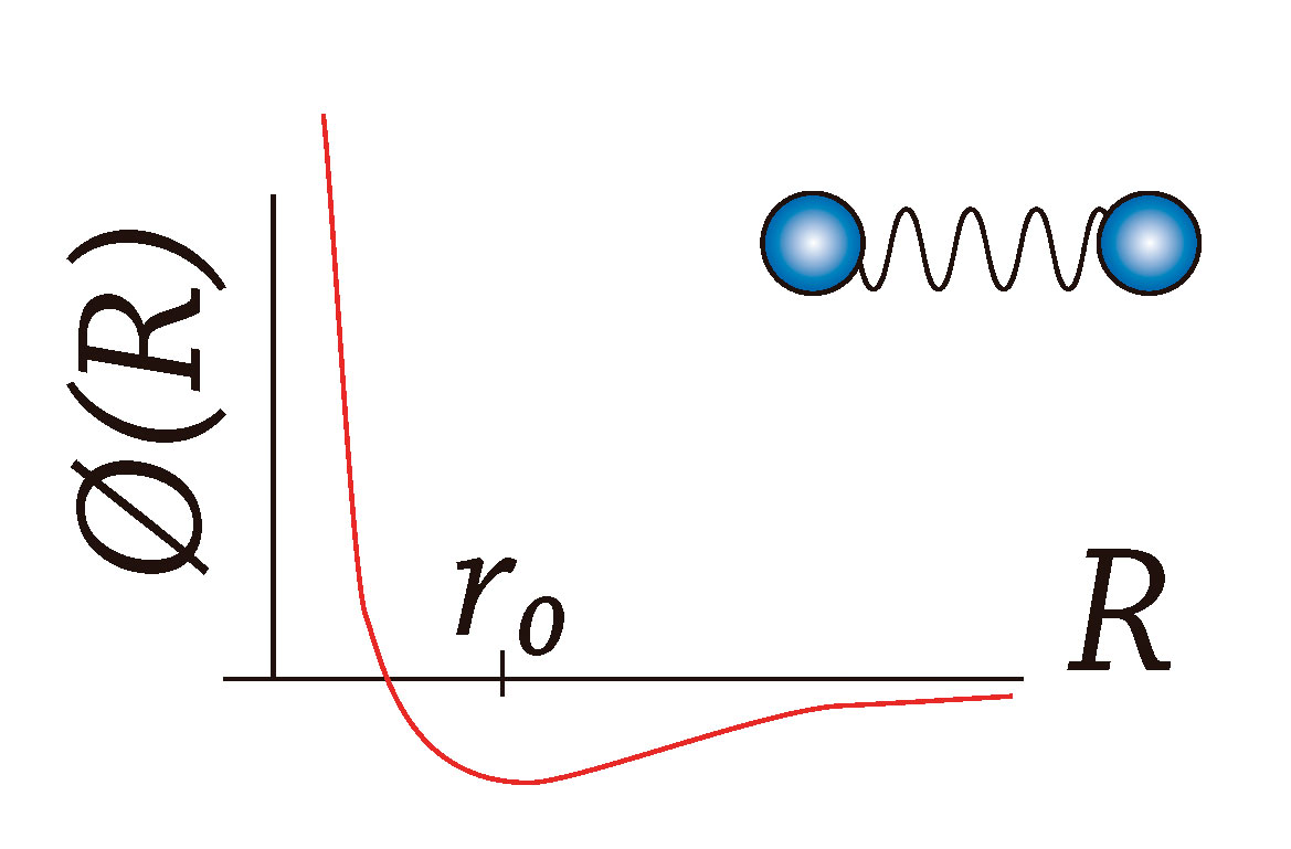
Figure 1 Schematic view of the interatomic potential. Distortions introduced from in an amorphous phase typically result in the lengthening of interatomic bond lengths.
In contrast to this behavior, the changes seen between the crystalline and amorphous phases of Ge2Sb2Te5 are unusually large. Collectively, Ge2Sb2Te5 and materials with similarly large differences between the crystalline and amorphous phases are often referred to as phase-change materials (PCM). An additional impetus for obtaining a deeper understanding of PCM in general and Ge2Sb2Te5 in particular, is that the large changes in electronic structure that Ge2Sb2Te5 experiences in the amorphous-crystalline phase transition also brings about a three order of magnitude decrease in resistivity. This large change along with the nanosecond scale timescale of the transition, make Ge2Sb2Te5 one of the most viable candidates for electrically based phase change memory PCRAM with the ultimately goal of achieving nonvolatile memory with DRAM like speeds and densities but, without the slow speed and limited lifetime of oxide-based FLASH memory.
Ge2Sb2Te5 is also unusual in that the crystalline phase used for recording purposes assumes a different, metastable structure than the equilibrium bulk hexagonal phase. While all of the previous statements form a good reason for trying to understand the switching mechanism in Ge2Sb2Te5, however, there are two additional factors that motivate in particular the use of synchrotron radiation. First, is the fact that the metastable and amorphous phases can only be formed in thin film form. In particular, the extremely large quench rates required for the amorphous phase with cooling rates in the range 108〜1012 K/s being reported necessary to generate the amorphous phase[8][8] C. Peng, L. Cheng and M. Mansuripur: "Experimental and theoretical investigations of laser-induced crystallization and amorphization in phase-change optical recording media" Journal of Applied Physics 82(9) 4183-4191, 1997.. This condition acts as a two edge sword, allowing very rapid write times, an attribute ideal for memory applications, but at the same time limits film thickness to a few tens of nanometers making analysis by conventional means more difficult. Second, is the fact that the amorphous phase is not readily observable using diffraction. X-ray absorption spectroscopy (XAFS) on the other hand is an elementally specific technique that allows examination of local order in both the amorphous and crystalline phases without additional complications due to coherence induced peak broadening. Fig. 2 shows a schematic diagram of the XAFS absorption process.

Figure 2 Schematic view of the x-ray absorption process in which an x-ray excites a core electron to the vacuum level in the form of a photoelectron. Backscattering from neighboring atoms of the outgoing photoelectron wavefunction gives rise to quantum mechanical interference and a concomitant oscillatory behavior in x-ray absorption with incident x-ray energy.
In XAFS, an incoming photon photo-excites a core electron to the vacuum level. The resulting outgoing photoelectron wavefunction is scattered by differences in the atomic potential from neighboring atoms and the backscattered contributions lead to quantum mechanical interference in the final quantum state. This quantum mechanical interference in turn leads to variations in the x-ray absorption cross section of the material being investigated due to the decrease that occurs in the photoelectron wavelength with increasing x-ray energy. The short (femotsecond order) lifetime of the core hole means that XAFS is an extremely fast process.
The same short lifetime of the core hole also limits the real-space distance probed from a few nanometers for photoelectron energies less than 〜40 eV (XANES region) to less than 1 nm for higher energies. This short coherence length allows the probing of both the amorphous and crystalline phases on a similar basis. The experimental quantity used as the starting point in XAFS analysis is χ(k) derived by subtracting the isolated atomic absorption from the observed changes in x-ray absorption with energy and converting to momentum k using the dispersion relation for appropriate for electrons. In XAFS, static and thermally induced displacements of interatomic distances are expressed in terms of a mean squared relative displacement factor which can be thought of as a two-site correlated Debye-Waller factor showing disorder along the bond direction. This is in contrast to the case of x-ray diffraction for which disorder as expressed by the Debye-Waller factor is about a single site.
2. Ge-Sb-Te Alloys
We have used XAFS to examine the local order about each constituent atom in both the crystalline and amorphous phases of Ge2Sb2Te5. Fig. 3 shows the realspace k2 weighted Fourier transform of the x-ray absorption signal χ(k) for the k-edges for each of the constituent elements. The χ(k) signal allows the realspace origin of the interference signal to be visualized and is somewhat analogous to a radial distribution function with a couple of caveats, first that as it is an interference function, destructive interference can give rise to dips or peaks in the spectra that are not due to the presence of atoms and second, the presence of a phase-shift in the wavefunction due to the presence of interatomic potentials results in a apparent shift in position to smaller r-values. Fig. 3 shows the Fourier transform of the k2 weighted χ(R) data for both crystalline (dotted) and laser-reamorphized (solid) Ge2Sb2Te5 for the k-edges of Ge, Sb, and Te[3][3] A. Kolobov, P. Fons, J. T. A. Frenkel, A. L. Ankudinov and T. Uruga: "Understanding the phase-change mechanism of rewritable optical media" Nature Materials 3 703-708, 10 2004.. It is apparent from the three spectra that there a systematic shift to shorter bond lengths in going from the crystalline to the amorphous phase. At the same time, the χ(R) data for all three edges indicates significantly, shorter nearest neighbor bond lengths for the amorphous phase versus the crystalline phase. While, powder x-ray diffraction studies have demonstrated that the average structure of the crystalline phase is rock-salt[12][12] N. Yamada and T. Matsunaga: "Structure of laser-crystallized Ge2Sb2+xTe5 sputtered thin films for use in optical memory" J. Appl. Phys. 88 7020-7028, 2000., a careful analysis of the XAFS data reveals the presence of Peierl distortion which results in the splitting of the Ge-Te and Sb-Te bonds into shorter and longer bonds[3][3] A. Kolobov, P. Fons, J. T. A. Frenkel, A. L. Ankudinov and T. Uruga: "Understanding the phase-change mechanism of rewritable optical media" Nature Materials 3 703-708, 10 2004.. Unlike x-ray diffraction, XAFS fringes are the direct result of quantum mechanical interference about a single site. The XAFS mean square displacement data also suggest the presence of a significant amount of possibly thermally induced disorder about the Ge atom site in particular reflecting the softness of the bonds to Ge[6][6] A. V. Kolobov, P. Fons, J. Tominaga, A. I. Frenkel, A. L. Ankudinov, S. N. Yannopoulos, K. S. Andrikopoulos and T. Uruga: "Why Phase-Change Media Are Fast and Stable: A New Approach to an Old Problem" Jpn. J. Appl. Phys. 44 3345−+, May 2005..
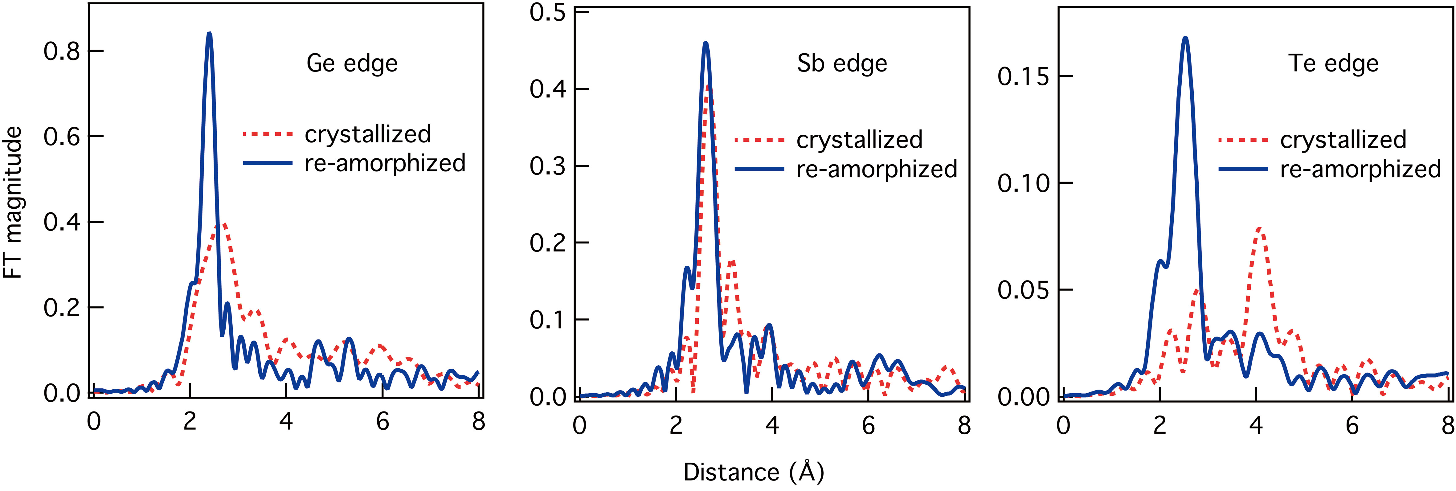
Figure 3 Experimental k2 weighted Fourier transforms of χ(R) for Ge, Sb, and Te K-edges in amorphous (solid) and crystalline (dotted) phases of Ge2Sb2Te5. Note that phase shift effects have not been removed from the data resulting in an apparent shift to smaller γ values. See text for details.
Unusually, the amorphous phase shows significantly less disorder and shorter bond lengths than the crystalline phase. The bond lengths as determined by XAFS show a value of 2.83 Å for the crystalline phase and 2.61 Å for the amorphous phase. These factors and others led Kolobov et al. to conclude that the local Te coordination of Ge atoms changes from a distorted octahedral to tetragonal upon the transformation from the crystalline to the amorphous phase[5][5] A. V. Kolobov, P. Fons, J. Tominaga, A. I. Frenkel, A. L. Ankudinov and T. Uruga: "Nanometer-scale mechanism of phase-change optical recording as revealed by XAFS" Nucl. Instrum. Methods B 246 69-74, May 2006.. Fig. 4 shows a schematic view of the local Te environment surrounding a Ge atom. For simplicity other atoms have been omitted from the figure and it should be noted that Ge atoms may have additional atoms near them other Te. It should also be noted that the formation of the amorphous phase is a stochastic process and this is a simplified picture. The aforementioned change in the local structural environment of Ge gives rise to characteristic changes in the near-edge structure (XANES region in Fig. 2); the collective nature of the scattering process in the XANES region and the increased distance probed captures characteristics of the three dimensional structure about the Ge atom.
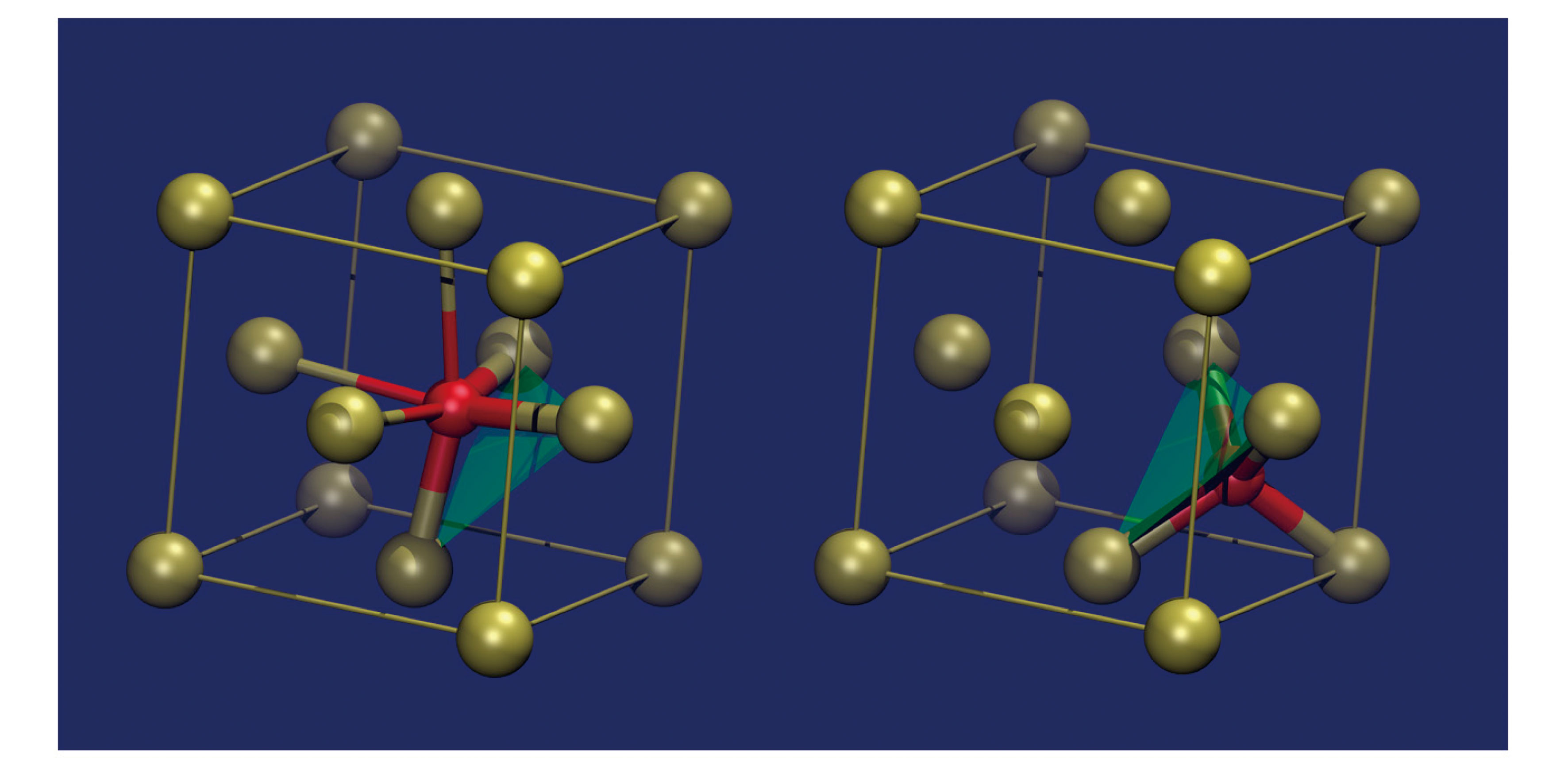
Figure 4 Simplified view of the local Te environment of Ge atoms in both the crystalline (left) and amorphous (right) phases of Ge2Sb2Te5. Only the local Te coordination has been shown and other atom types have been omitted for simplicity.
3. Experiment
Optical experiments in which a pump laser induces changes in a layer of phase-change material while a second, lower intensity laser probes changes in optical constants have shown characteristic switching times as low as 50 ns for Ge2Sb2Te5[9,10][9] C. B. Peng and M. Mansuripur: "Amorphization induced by subnanosecond laser pulses in phase-change optical recording media" Appl. Optics 43 4367-4375, AUG 1 2004.
[10] S. Raoux, R. Shelby, B. Munoz, M. Hitzbleck, D. Krebs, M. Salinga, M. Woda, M. Austgen, K.-M. Chung and M. Wuttig: "Crystallization Times of As-deposited and Melt-quenched Amorphous Phase Change Materials" In Proc. Europ. Symp. On Phase Change and Ovonic Science 2008.. It is also important to note that the crystallization time of the laser reamorpized phase is significantly faster than that of as-deposited sputtered material; significant differences in local order have also been reported between as-deposited and as-sputtered Ge2Sb2Te5[1][1] P. Fons: Phase Change Materials: Science and Applications chapter 8 pages 141-173. Springer Verlag, 2008.. Somewhat more unclear is the origin of differences in optical pump-probe observations observed by different groups, a fact compounded by the complicated and multiple origins of optical properties. While phenomenological changes can be observed using optical pump-probe techniques, the underlying changes in structure that ultimately give rise to the optical changes are more obscure. To address this knowledge deficit, we have applied synchrotron-based time-resolved XAFS. There are several advantages in using synchrotron based XAFS techniques to time resolve the changes occurring during optically induced switching in phase-change materials. First, XAFS allows probing of the local structure of the amorphous and crystalline phases on an equal basis without concern for coherence length effects that alternative spectroscopies such as diffraction suffer from. Second, the time-structure of x-ray generation of a synchrotron is well matched to the hundreds of picosecond time scale of the phase-change transition process. In a synchrotron, x-rays are generated as a consequence of (angularly) accelerated electrons in a storage ring. The electron bunch structure in a synchrotron is defined by the storage ring lattice; only electrons that are synchronous with the electrodes in the RF acceleration cavity receive energy each pass causing the electrons in each bunch to have a well defined energy and hence orbital speed. While an electron bunch is accelerated due to a magnetic field, an x-ray pulse is generated. For SPring-8, this leads to an orbit time of 4790 ns (208.73 kHz) for a single bunch and a corresponding bunch duration of about 40 ps; the generated x-ray pulses have the same time structure as the electron bunch. Typical optical pump/probe experiments introduce an additional path to provide a temporal delay for a probe beam split off from the pump beam to maintain synchronization. For synchrotron based experiments, however, the period between x-ray bursts is determined by the orbit time around the storage ring of an electron bunch. The synchrotron thus must serve as the ultimate time base for any pump probe experiment. The current experiment was developed and carried out at SPring-8 using beamline BL39XU. The beamline is equipped an standard in-vacuum undulator with a (111) diamond double crystal diffractometer. Higher harmonic rejection is achieved using a Rh-coated mirror. An x-ray microbeam was generated using a Kirpatrick-Baez mirror fabricated from Si; the mirror has an estimated flux of 1 × 10¹⁰ photons/second for approximately a 1µm diameter x-ray beam[11][11] M. Takagaki, M. Suzuki, N. Kawamura, H. Mimura and T. Ishikawa: "Development of scanning hard x-ray microprobe for element-specific magnetic imaging at SPring-8 BL39XU" Proc. 8th Int. Conf. X-ray Microscopy 7 267-269, 2005.. The experiment was typically operated in a hybrid mode in which the average current in the bunch used for the experiment was between 2-3 mA. Fig. 5 shows the schematic layout of instrumentation used for the experiment[2][2] P. Fons, A. V. Kolobov, T. Fukaya, M. Suzuki, T. Uruga, N. Kawamura, M. Takagaki, H. Ohsawa, H. Tanida and J. Tominaga: "Sub-Nanosecond Time-Resolved Structural Measurements of the Phase-Change Alloy Ge2Sb2Te5" Jpn. J. Appl. Phys. Part I 46 3711-3714, June 2007..
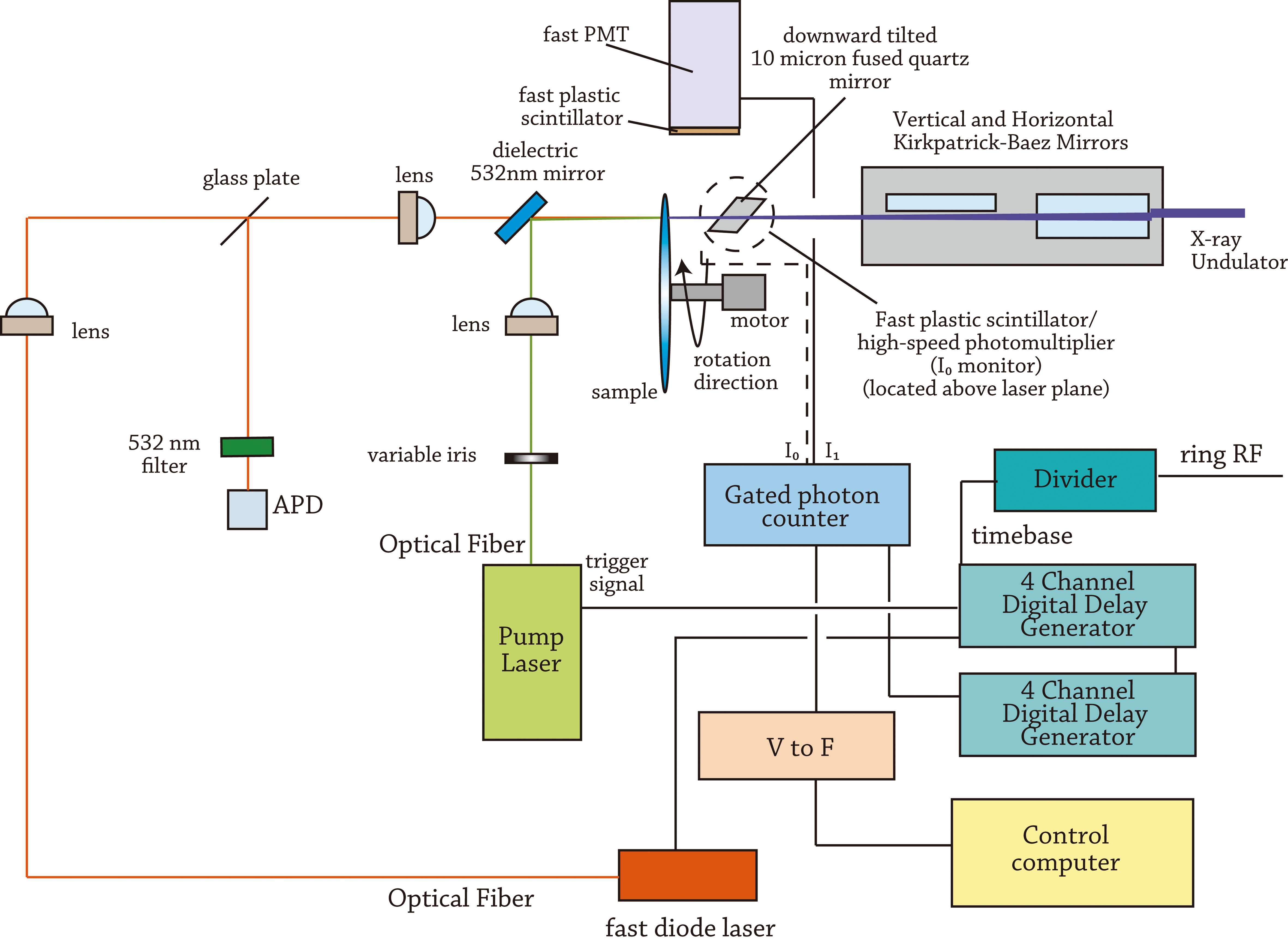
Figure 5 Schematic of the instrumentation layout used for the time-resolved experiments.
4. Timing
As the RF signal used to compensate for energy losses of electrons as they transit the ring is intrinsically phase locked to the temporal position of the x-ray pulses, the time base for the current experiment was derived from a suitably divided down signal generated from the RF signal used by the ring; in these experiments, the laser was triggered at a frequency of approximately 50 kHz. This signal was then introduced into a digital delay generator. To compensate for propagation time offsets for both the optical pump and the x-ray probe pulses, their relative position was assessed using an avalanche photo diode (APD) that could detect both x-ray and pump photons and the offsets were adjusted accordingly. The delay generator has two output channels each of which can be delayed by a user settable values in 10 ps increments. One output was directed to the trigger electronics of the pump laser, while a second served as a trigger signal for a multichannel gated photon counter. Using this signal the two channels of the gated photon counter integrated the incident beam I0 and fluorescence I signal intensities. A thin amorphous silica plate served as a scattering source to monitor the intensity I0 of the particular bunch used for the pump-probe experiment. A second delay generator was used to trigger two additional channels in the gated photon counter to monitor both I0 and I for the same electron bunch exactly one orbit earlier. The x-ray absorption signal was thus continuously monitored both with and without the pump laser. The baseline signal obtained in this manner provided conclusive evidence that the changes observed were indeed to the pump laser. The use of a nanosecond window for the photon counter provided robust insensitivity to background noise as the counter only operates when there is an XAFS signal to be measured; the detector signal is only used when there is a corresponding laser pump pulse. The local structure around Ge atoms in Ge2Sb2Te5 was probed in these initial experiments using the Ge K-edge (11.1 keV). Ge K-α fluorescence photons were converted to visible light using a fast plastic scintillator with a 〜1 ns rise time which was then in turned into an electrical signal using a fast photomultiplier. An additional digital delay generator was used to trigger an optical probe laser to provide optical data taken simultaneously with the x-ray probe experiment.
In our optical-pump/x-ray probe experiments, we used a Ge2Sb2Te5 sample grown on an optically flat silica disk which was rotated at a speed sufficient to avoid the 20 µm pump laser spot size falling in the same spatial location for two sequential pulses. The x-ray probe beam was about 2-3 µm in size and was directed anti-parallel to the optical pump beam to minimize the effects of jitter in the ultra low wobble sample mount. A second CW recrystallizing laser was directed towards the sample such that it was incident on the same circular arc as the amorphization laser ensuring that the Ge2Sb2Te5 was re-crystallized before the amorphization pulse of the optical pump laser hit the sample. Fig. 6 shows a fluorescence map taken using the 〜1-2 µm x-ray beam with the monochromator fixed at the white line position. As the relative white line intensities of the laser re-crystallized, as-deposited, and re-amorphized regions decrease in order, the relative sizes of the different regions can be clearly seen in the figure. The x-ray probe beam was slightly less than the size of a single pixel in the image.
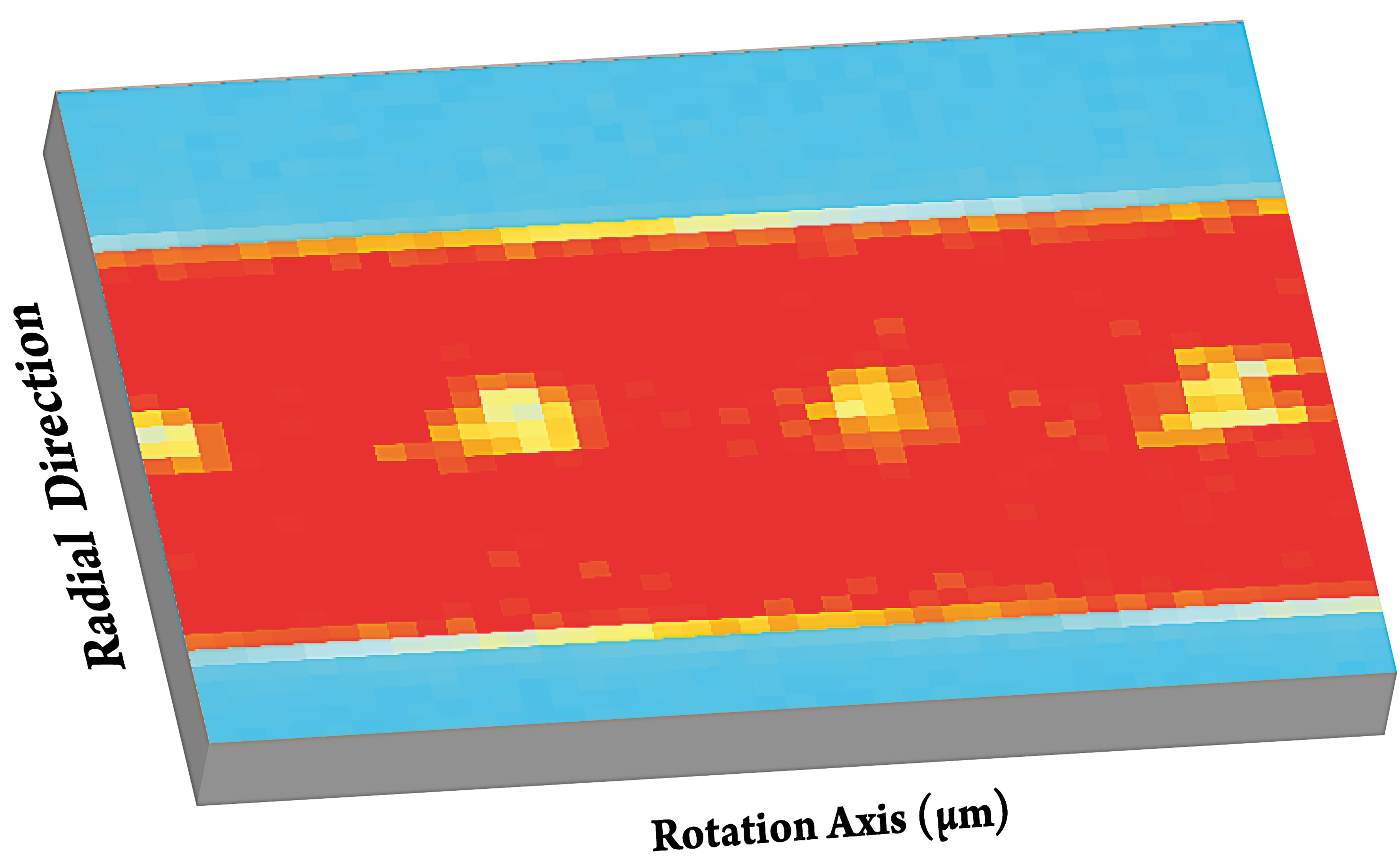
Figure 6 Ge x-ray fluorescence map taken with the monochromator fixed at the white line position (E〜11103 eV). In the figure, the as-deposited (blue), laser re-crystallized (red), and laser re-amorphized (yellow) regions can be seen.
5. Experiment
In the experiment, a pump laser with a duration of 600 ps was chosen as it gives rise to a similar excitation process as that which occurs in optical memory recording. The pump pulse is sufficiently long that the excitation process can be thought of as inducing predominately thermal processes although the fact that Ge2Sb2Te5 is a semiconductor[7][7] B.-S. Lee, J. R. Abelson, S. G. Bishop, D.-H. Kang, B.-K. Cheong and K.-B. Kim: "Investigation of the optical and electronic properties of Ge2Sb2Te5 phase change material in its amorphous, cubic, and hexagonal phases" J. Appl. Phys. 97 3509−+, 2005 implies that the large photon density present during excitation may lead to possible preferential bond breaking effects[4][4] A. Kolobov, P. Fons and J. Tominaga: "What makes phase-change chalcogenide alloys materials of choice for optical data storage" Proc. Mat. Res. Soc. 918E H04-05, 4 2006.. XAFS spectra were collected to approximately 12 Å-1 by fixing the delay between the excitation laser and the probe x-ray pulse and then step scanning the monochromator from approximately 100 eV below to 〜600 eV above the edge. At each energy point spectra, were integrated for a fixed delay until sufficient signal to noise was achieved. A typical scan required about 80 minutes to complete. The maximum current in the electron bunch used varied from approximately 2-3 mA depending on fill mode.
The relative delay of the x-ray probe to the pump laser was varied over 250 ps steps in the vicinity of time t = 0. Fig. 7 shows some typical k2 weighted Fourier transforms of χ(R) data calculated using the k-range 2-8 Å for a few different delays. The re-crystallized (blue) and re-amorphized (yellow) traces represent the starting and ending points of the transition from the crystalline to amorphous state.
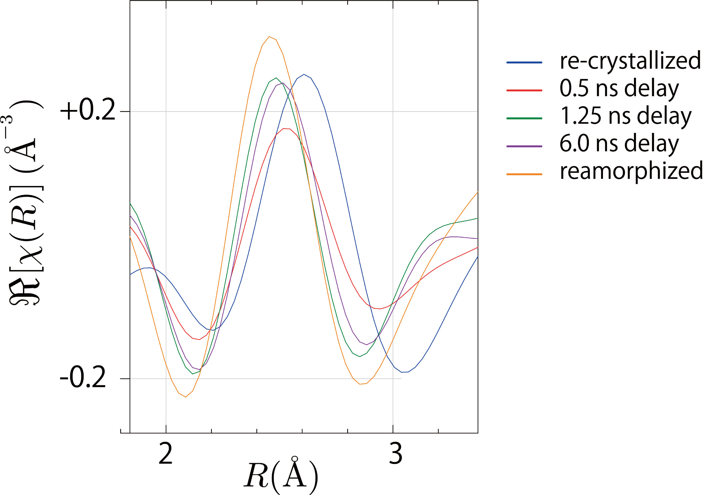
Figure 7 k2 weight χ(R) data for various probe times ranging as well as standard laser re-crystallized and re-amorphized spectra taken using the same apparatus.
6. Conclusion
Using the above procedure, we have shown that it is possible to time resolve structural data on the hundreds of picosecond time scale of the optical recording process. The approach taken here is general and as lasers are used for the heating part of the process, the same general approach can be used to investigate the effects of extreme temperatures and/or pressures in a wide variety of materials. In the current experiment, the thickness of the sample was limited to 50 nm of thickness due to the limited ability of the pump light to penetrate. This corresponds to approximately 8 unit cells of Ge2Sb2Te5 or an equivalent of three monolayers of Ge demonstrating the sensitivity of the approach. Our group is currently in the process of analyzing the details of the data in the context of finite element calculations of the temperature dynamics. Further details will be published elsewhere.
Bibliography
[1] P. Fons: Phase Change Materials: Science and Applications chapter 8 pages 141-173. Springer Verlag, 2008.
[2] P. Fons, A. V. Kolobov, T. Fukaya, M. Suzuki, T. Uruga, N. Kawamura, M. Takagaki, H. Ohsawa, H. Tanida and J. Tominaga: "Sub-Nanosecond Time-Resolved Structural Measurements of the Phase-Change Alloy Ge2Sb2Te5" Jpn. J. Appl. Phys. Part I 46 3711-3714, June 2007.
[3] A. Kolobov, P. Fons, J. T. A. Frenkel, A. L. Ankudinov and T. Uruga: "Understanding the phase-change mechanism of rewritable optical media" Nature Materials 3 703-708, 10 2004.
[4] A. Kolobov, P. Fons and J. Tominaga: "What makes phase-change chalcogenide alloys materials of choice for optical data storage" Proc. Mat. Res. Soc. 918E H04-05, 4 2006.
[5] A. V. Kolobov, P. Fons, J. Tominaga, A. I. Frenkel, A. L. Ankudinov and T. Uruga: "Nanometer-scale mechanism of phase-change optical recording as revealed by XAFS" Nucl. Instrum. Methods B 246 69-74, May 2006.
[6] A. V. Kolobov, P. Fons, J. Tominaga, A. I. Frenkel, A. L. Ankudinov, S. N. Yannopoulos, K. S. Andrikopoulos and T. Uruga: "Why Phase-Change Media Are Fast and Stable: A New Approach to an Old Problem" Jpn. J. Appl. Phys. 44 3345−+, May 2005
[7] B.-S. Lee, J. R. Abelson, S. G. Bishop, D.-H. Kang, B.-K. Cheong and K.-B. Kim: "Investigation of the optical and electronic properties of Ge2Sb2Te5 phase change material in its amorphous, cubic, and hexagonal phases" J. Appl. Phys. 97 3509−+, 2005
[8] C. Peng, L. Cheng and M. Mansuripur: "Experimental and theoretical investigations of laser-induced crystallization and amorphization in phase-change optical recording media" Journal of Applied Physics 82(9) 4183-4191, 1997.
[9] C. B. Peng and M. Mansuripur: "Amorphization induced by subnanosecond laser pulses in phase-change optical recording media" Appl. Optics 43 4367-4375, AUG 1 2004.
[10] S. Raoux, R. Shelby, B. Munoz, M. Hitzbleck, D. Krebs, M. Salinga, M. Woda, M. Austgen, K.-M. Chung and M. Wuttig: "Crystallization Times of As-deposited and Melt-quenched Amorphous Phase Change Materials" In Proc. Europ. Symp. On Phase Change and Ovonic Science 2008.
[11] M. Takagaki, M. Suzuki, N. Kawamura, H. Mimura and T. Ishikawa: "Development of scanning hard x-ray microprobe for element-specific magnetic imaging at SPring-8 BL39XU" Proc. 8th Int. Conf. X-ray Microscopy 7 267-269, 2005.
[12] N. Yamada and T. Matsunaga: "Structure of laser-crystallized Ge2Sb2+xTe5 sputtered thin films for use in optical memory" J. Appl. Phys. 88 7020-7028, 2000.


