


Volume6 No.2
SPring-8 Section A: Scientific Research Report
HAXPES Study of Multilayer Oxidation Films on Si(100)
National Tsing Hua University
- Abstract
-
We have carried out hard X-ray photoemission spectroscopy (HAXPES) measurement of the multilayer oxides on the Si(100) surface. Despite of many difficulties, we were able to acquire some data which provides us some further understanding of these buried oxide layers.
Keywords: oxides, silicon, hard X-ray photoemission spectroscopy
Background and Purpose
In many practical applications such as those in the solar cells and high-end semiconductor chip fabrications, multilayer stacks each in the range of a few nanometers are often employed for best efficiency or optimized speed. Figure 1 shows an example of high-k metal gate stacks that was used in Intel’s 45 nm microprocessors. The interfacial properties between the silicon and the high-k dielectric film is ~2 nm in thickness and the effect on the dielectric films upon the deposition of the work function metal plays an important role in the device characteristics and performances.
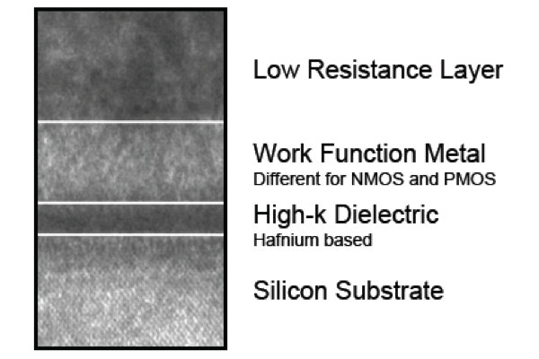
Figure 1. High-k Dielectric and Metal Gate Transistor Stack
Synchrotron photoemission spectroscopy (SPES) is a powerful tool for investigating the electronic and atomic structure of solids. Due to the limits of analyzers and beamlines performance, photoelectrons with kinetic energies typically around 10-1000 eV are examined. The electron escape depth ranges from a few angstroms to a couple of nanometers. Traditional SPES thus provides information on several topmost atomic layers. The electron escape depth gets larger as the kinetic energies increases. Hence bulk-sensitive information can be obtained in photoemission experiments only if high-energy electrons are detected.
Experimental Summary
Growing a good oxide layer on the MOSFET device is an important issue. With decreasing of the device size, the thickness of oxide layer is also reduced. How does the gate have a good switch ability with the ultra-thin oxide layer? Therefore, the high-K material (HfO2) is applied. According to the previous literature,[1] there must have a buffer layer between the HfO2 and silicon bulk, which is silicon dioxide layer. We had several difficulties: the prepared samples were not perfect, the beamtime was only three days, and the experimental apparatus was complex and new to us. Despite these problems, we got some data, but they were not enough to make a complete analysis to obtain a solid conclusion.
Result and Discussion
In situ growth of these high quality multilayer films on a research-based synchrotron facility is often non-practical. With the availability of intense photon fluxes tunable at 2 keV up to 12 keV photons with a resolution down to less than 100 meV and analyzers now able to measure large photoelectron energies, hard X-ray photoemission spectroscopy can be a non-destructive depth profiling technique, which allows measurements of thick epitaxial layers and deeply buried interfaces.
Here the layer structure of the sample we obtained from our collaborators is as followed: HfO2 (1.9 nm)/SiO2 (~0.5 nm)/Si (1 nm)/SiGe (7.5 nm)/Si(100) bulk + NH3 anneal. Combined chemical vapor deposition and atomic layer epitaxy (CVD/ALE) methods are employed to grow these films. The photoemission spectra for the Si 1s, O 1s, and Ge 3d are shown in Figs. 2 and 3. The line shapes and chemical shifts of these spectra are similar to previous reports.[1,2,3] Intensity plots obtained from analysis for various core levels are shown in Fig. 4. It is clear that the intensities of signals from the thin film increase with emission angles except for the Si 1s from the bulk. Thus, it is possible to estimate the average depth of the corresponding elements from the degree of intensity rises or decreases.
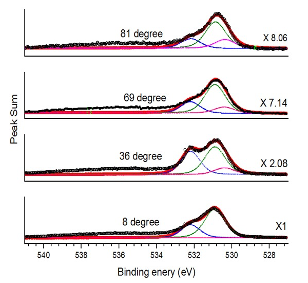
Figure 2. Photoemission spectra and their decomposition for O 1s core-levels from various angles.
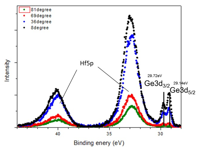
Figure 3. Photoemission spectra for Ge 3d core-levels from various angle as indicated.
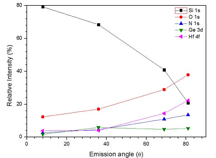
Figure 4. Intensity plots obtained from analysis for various core levels. The intensities increase with emission angles except for the Si 1s from the bulk.
The samples of the first classification are too thin to detect the high resolution signal because the most photoemission spectroscopy signal come from the silicon bulk. The signal of the surface oxide are buried. But, the second classification of high-K material film were detected successfully for the different depth layer. By the core level shift signal, we can deduce the atom bonding status of the film. Depending on different preparation process of the sample, the interface bonding status is different. This information shows the oxidation state of the different depth film.
Challenges
We have employed the HAXPES technique to study the complex multi-layer high-K materials. Although some useful data were obtained as the principle of the technique predicted, however, the end station and the sample manipulation during the data taking is very complex, requiring more than three skilled personal support in addition to the outside researchers. Without these supports, carrying out experiment is difficult and inefficient. As for the sample, the cost of making the multilayer samples is too high. Now the collaborator is unable to provide more controllable samples, and thus, we won’t be able to continue this research.
References:
[1]: Nobuyuki, F., et al., Jpn. J. Appl. Phys. 56, 04CB04 (2017)
[2]: Yasuhiro, A., et al., Jpn. J. Appl. Phys. 48, 041201 (2009)
[3]: Rubio-Zuazo, J., and Castro, G. R. Journal of Vacuum Science & Technology A, 31, 031103 (2013)
ⒸJASRI
(Received: March 17, 2017; Early edition: May 30, 2018; Accepted: July 3, 2018; Published: August 16, 2018)