


Volume4 No.2
SPring-8 Section A: Scientific Research Report
Analysis of Electronic States of New Solution-processed, Unusual P-type Oxides by Using Hard X-ray Photoelectron Spectroscopy (HXPES)
aJST-ERATO, Shimoda Nano-Liquid Process Project, 2-13 Asahidai, Nomi, Ishikawa 923-1211, Japan
bGreen Devices Research Center, Japan Advanced Institute of Science and Technology, 2-13 Asahidai,Nomi, Ishikawa 923-1211, Japan
cSPring-8 / Japan Synchrotron Radiation Research Institute, Sayo, Hyogo, 679-5198 Japan
dSchool of Materials Science, Japan Advanced Institute of Science and Technology, 1-1 Asahidai, Nomi, Ishikawa 923-1292, Japan
- Abstract
-
Our unusual p-type oxide, Ni-Rh-O, showed unprecedentedly low resistivity (10-4 – 10-5 ohm cm) and metallic conduction. HXPES indicated nickel in the Ni2+ state while rhodium mainly in the Rh0 state, suggesting a phase composition of Rh5.14(NiO)(Rh2O3)0.13C0.16. A Rh0 core-oxide shell-structure was proposed to explain the unusual conduction properties.
Keywords: Ni-Rh-O, p-type, electronic state
Background and Research Purpose
We have been studying direct printing of metal oxide materials and devices [1], during which we have synthesized a series of new p-type oxides of transition metals from simple solution processing [2-4]. Among these oxides is Ni-Rh-O that shows unusual properties (unprecedentedly low resistivity (10-4 – 10-5 ohm cm) and metallic conduction instead of semiconducting behavior) and is processable at low temperatures (≤400°C). More specifically, the Ni-Rh-O is highly conductive with the carriers being holes as found in the Hall-effect measurement and its resistivity decreased linearly with the decrease of sample temperature. The resistivity is over one order lower than the ever known p-type oxide of low resistivity (Cu-based oxide by vacuum deposition, 10-3 ohm cm, annealed at 1000°C), which is potential for applications in hole injection electrodes and hole transport.
The material was synthesized in several steps, with elemental composition, structure, and conducting properties varying in each step. First, the precursor solution was spin-coated on an insulating substrate and annealed below 300°C, giving a p-type amorphous semiconductor working as a p-channel in a thin-film transistor. Second, the film was reduced using hydrogen radicals (H*) below 100°C, resulting in a n-type nanocrystalline material with metallic conduction and having a typical composition of NiRh0.94(2)O0.13(6)H0.12(2)C0.12(2) for Ni/Rh =1, where values in parentheses are uncertainties to the last digits (hereafter same). Third, the film was re-oxidized, e.g., at 400°C, converting it to a p-type nanocrystalline material with metallic conduction and having a typical average composition of NiRh0.95(3)O1.07(8)C0.06(2) for Ni/Rh = 1.0. The n-type to p-type conversion occurred within a few minutes in the re-oxidation. The unusual material mentioned above refers to this re-oxidized one after this final step, which is the targeted material of this analysis.
Elemental analysis combined with high-resolution transmission electron microscopic (HRTEM) observations showed that during re-oxidation, the material separated into two layers, with the upper one being nanocrystalline NiO (typical composition NiO1.00(6)C0.04(1)) and the lower one being a Rh-rich and oxygen-poor Ni-Rh-O oxide (typical composition NiRh5.4(3)O1.4(2)C0.16(5)), for Ni/Rh = 1.0 (around 25 nm thick upper layer and 25 nm thick lower one for a 50 nm thick film). Electron diffraction for the lower layer showed only the Rh2O3 structure, and thus TEM analysis in more details may be necessary. We also prepared films with Ni/Rh = 1.0/5.4 in the starting solution, of which the metal composition was the same as in the above lower layer, and found the similar conducting properties. Of the two layers, only the Rh-rich oxide layer can be responsible for the unusual properties.
HXPES at SPring-8 was performed to detect the bulk electronic states of the Ni-Rh-O in order to give insight into the physics of the unusual properties. Common lab-XPS and UPS were not used because these methods are only surface sensitive and merely detect the NiO layer. Etching through Ar ion sputtering can expose the lower layer, but it also reduces the rhodium from Rh3+ to Rh0 and changes the electronic states.
Experimental Summary
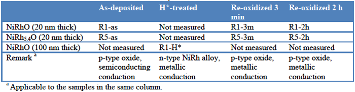
The solution (metal acetates and propionic acid) was spin-coated on SiO2/Si substrates. The films were annealed at 270°C, and then H*-treated below 100°C in a radical treatment system. Here H* represents hydrogen radicals and was obtained by passing H2 through a high-temperature (>1600°C) tungsten filament. Thereafter, the films were re-oxidized at 400°C on a ceramic hotplate in air. Samples of both Ni/Rh = 1.0 and 1.0/5.4 in the solutions were prepared. The samples measured for HXPES were listed in Table 1. NiO and Rh2O3 reference samples were prepared from corresponding solutions and annealed at 550°C in oxygen. HXPES was performed at BL47XU at a photon energy of 7940 eV. An Au standard sample was used for calibration of the energy in the HXPES system. A detecting angle of 89° to the normal of the sample surface was used in order to reduce the signal from the substrate while an angle of 30° was also applied for some measurements for the purpose of confirmation of the substrate signal. In addition, the elemental compositions of the films were all obtained using a combinational Rutherford Backscattering Spectrometry (RBS), Nuclear Reaction Analysis (NRA) and Hydrogen Forward Scattering Spectrometry (HFS) on Pelletron 3SDH (National Electrostatics Corp.) at Toray Research Center, Inc., Japan, with estimated precisions of ±0.5 atom% for C and H, ±1 atom% for Ni and Rh, and ±4 atom% for O. The carrier type and semiconducting or metallic conduction were evaluated using Hall-effect measurement, temperature-dependence measurement of resistivity (Physical Property Measurement System, PPMS, Quantum Design), as well as thin-film transistors with Ni-Rh-O being the channel, and the results are summarized in Table 1.
Table 1. Sample names for HXPES
Results and Discussion
Fig. 1 shows the valence band spectra of HXPES. (Note that the data were re-scaled by multiplying coefficients to give the same maximum height in this and other figures.) The binding energy (BE) at 0 eV corresponds to the Fermi level. The VBM (valence band maximum) was composed of the Rh 4d and Ni 3d orbitals, which hybridized with deeper O 2p. The as-deposited samples (R1-as and R5-as) had their VBM 0.4-0.5 eV below the Fermi level, which was consistent with their p-type semiconducting properties. After H*-treatment (sample R1-H*), the VBM was over the Fermi level, which corresponded to the n-type and metallic properties. After re-oxidation (R1-3m, R1-2h, R5-3m, R5-2h), the valence band near the Fermi level decreased, but the VBM was still over the Fermi level. The decrease of the valence band near the Fermi level is attributed to the decrease in the amount of metals in the reduced states (Ni0 and Rh0) after re-oxidation. According the elemental compositional analysis, the H*-treated sample for Ni/Rh = 1 (sample R1-H*) had a composition of NiRh0.94(2)O0.13(6)H0.12(2)C0.12(2), being a nanocrystalline plus amorphous NiRh metal alloy (TEM and electron diffraction analyses). It changed to NiRh0.95(3)O1.07(8)C0.06(2) after re-oxidation for 2 h (sample R1-2h). A VBM over the Fermi level indicated that free electrons were available and the conduction should be metallic even after re-oxidation, which was consistent with temperature-dependence measurement of resistivity that showed linear increase in resistivity with increasing sample temperature. However, the p-type behavior (hole conduction) could not be explained.
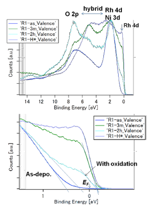

Fig. 1. Valence band spectra of HXPES. (left) NiRhO, (right) NiRh5.4O. The lower panels are enlarged from the upper ones to show the details near the Fermi level (BE = 0).
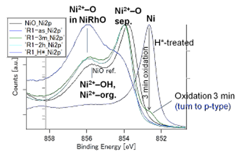
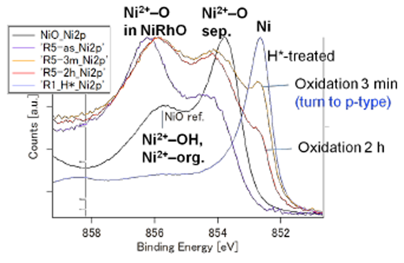
Fig. 2. HXPES spectra of Ni 2p 3/2. (left) NiRhO, (right) NiRh5.4O. Ni2+-OH and Ni2+-org. indicate Ni2+ ions bonded to OH- groups and organic carboxylate ligands (RCOO-), respectively. Ni2+-O sep. represents Ni2+ ions in the separated NiO phase.
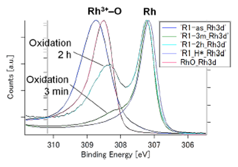
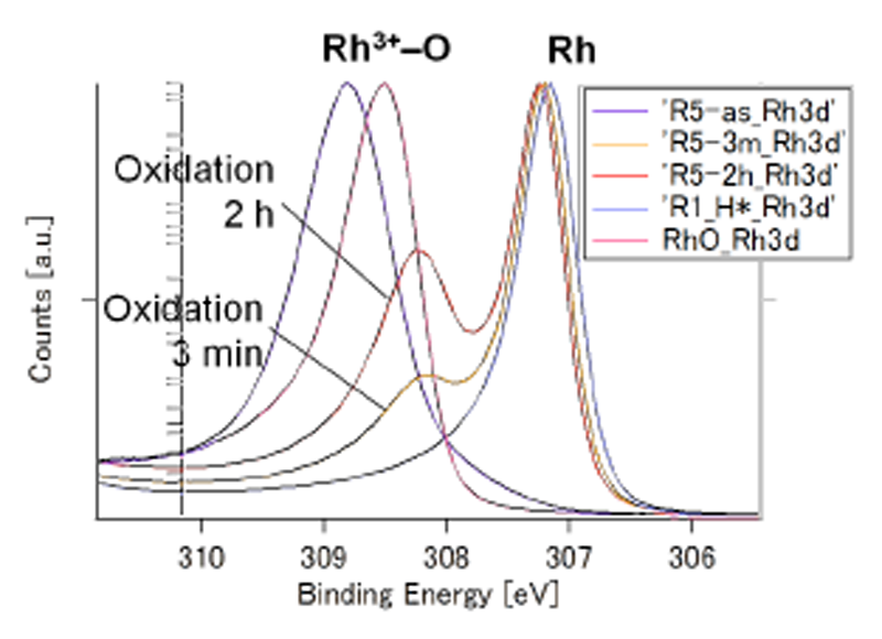
Fig. 3. HXPES spectra of Rh 3d 5/2. (left) NiRhO, (right) NiRh5.4O
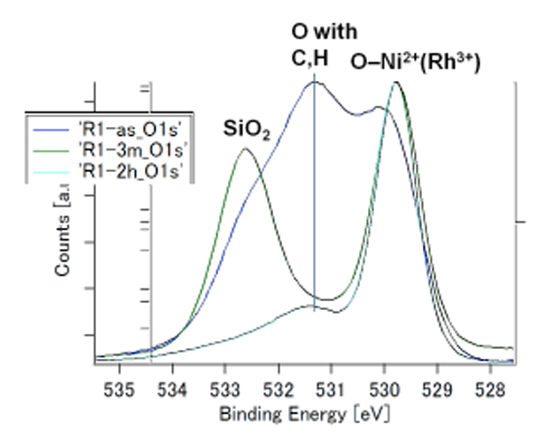
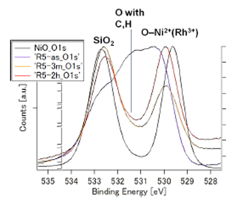

Fig. 4. HXPES spectra of O 1s. (upper left) NiRhO, (upper right) NiRh5.4O. The lower panel shows comparison of spectra of the R1-2h sample, detected at 89° (black) and 30° (red), respectively, to the normal of the sample surface. Photoelectrons from deeper O atoms were detected at 30°. This confirmed the assignment of the peak at BE ~532.7 eV to O in substrate SiO2.
Fig. 2 presents the Ni 2p 3/2 spectra of the samples and a NiO reference. The as-deposited sample has nickel at its oxidized state Ni2+, and the H*-treatment reduced it to the metal state (Ni0). In NiRhO samples, after only 3 min of re-oxidation, the Ni0 line has become minor in contrast with the strong lines of the oxidized state Ni2+. The Ni0 line further decreased or disappeared with longer re-oxidation time. In contrast, in NiRh5.4O samples, even after re-oxidation for 2 h, a minor nickel in the metal state was still observed. This minor Ni0 is considered to be remained in Rh0 crystals, forming a stable alloy structure that was resistant against oxidation. In the NiRhO samples, such minor Ni0 was not detected, probably because that its relative amount compared to Ni2+ was too small to be found.
Fig. 3 displays the Rh 3d 5/2 spectra of the samples and a Rh2O3 reference. The as-deposited and H*-treated samples showed rhodium at the oxidized (Rh3+) and reduced (Rh0) states, respectively, similar to those of nickel. However, in contrast to nickel, re-oxidation has little effect on the intensity of the Rh0 line. Only a minor Rh3+ line appears after 3 min of oxidation, and its intensity is much lower than that of the as-deposited sample even after 2 h of re-oxidation.
Fig. 4 shows the O 1s spectra. The line attributed to SiO2 was confirmed by changing the detecting angle, as shown in the lower panel of Fig. 4 (see also the caption of this figure). It is noted that in the R1-2h sample, O 1s peak from SiO2 was absent at a detection angle of 89° (to the normal of the sample surface), unlike other samples. The reason is unclear at present. The reproducibility may need to be confirmed before finding the reason. In the NiRh5.4O samples, the O 1s band for O atoms bonded to Ni and Rh enhanced with the increase in the re-oxidation time from 3 min to 2 h, as consistent with the variation of the Ni 2p 3/2 and Rh 3d 5/2 bands observed above. In the NiRhO samples, the evolution of the O 1s band could not be analyzed because of the lack of a reference SiO2-originated O 1s band.
According to the HXPES data and other compositional and structural analysis described in the first section, it is clear that the p-type, highly conductive, and metallic Ni-Rh-O, which is Rh-rich (Ni/Rh = 1.0/5.4) and O-poor, is a mixture of Rh metal (Rh0) and oxides of Ni and Rh. The typical composition after several hours of re-oxidation, NiRh5.4(3)O1.4(2)C0.16(5), may be re-written as Rh5.14(NiO)(Rh2O3)0.13C0.16. The Rh0 is the major component, the content of which is several times higher than that of the minor oxides. In the samples that has been re-oxidized for only 3 min, the content of oxides must be even lower. Accordingly, it is proposed that in re-oxidation, a Rh0 core-oxide shell-structure was formed, with the major Rh0 isolated by the minor oxide phases. The oxides existed just like a boundary phase. In other words, Rh0 grains were each surrounded by the minor oxide phases that formed a thin intergranular layer and were continuous all through the whole material. Since these oxides are p-type, holes can transport all through the whole material while electrons are restricted in the isolated Rh0. As a result, a Hall-effect measurement shows p-type (hole) conduction. On the other hand, the conductivity of the whole material may be dominated by the major metal phase, leading to a metallic conduction.
Because HXPES is sensitive to the bulk instead of the surface, the VBM band over the Fermi level after re-oxidation originated from the core rhodium remaining in the reduced metal state (Rh0). The VBM band of the oxides near and below the Fermi level was hidden by this VBM band of Rh0.
Challenges
In order to clarify the structure in details, i.e., the distribution relationship of Rh0 and oxides, more thorough HRTEM should be performed, which seems to be a challenge since previous HRTEM even failed in finding Rh0. In addition, modeling of the structure for simulating the conduction is necessary for a convincing explanation of the unusual conduction.
Acknowledgements
We thank Dr. Yoshitaka Murakami, Dr. Daisuke Hirose, and Mr. Hirokazu Tsukada for assistance in the HXPES experiment. This work was financially supported by Japan Science and Technology Agency through JST-ERATO Shimoda Nano-Liquid Process Project.
References
[1] T. Kaneda, et al. J. Mater. Chem. C 2, 40 (2014).
[2] J. Li, et al. Appl. Phys. Lett. 101, 052102 (2012).
[3] J. Li, et al. Appl. Phys. Lett. 101, 132104 (2012).
[4] T. Shimoda and J. Li, Patent application No. PCT/JP2013/056207 (2013).
ⒸJASRI
(Received: December 7, 2015; Early edition: February 25, 2016; Accepted: June 24, 2016; Published: July 25, 2016)