


Volume4 No.1
SPring-8 Section A: Scientific Research Report
In-Situ Studies of Polytypic Formation and Reconstructions in Selected Area Grown III-V Heterostructures on Silicon
aNiels Bohr Institute, University of Copenhagen, Denmark
bCenter for Quantum Devices and Station Q Copenhagen, Niels Bohr Institute, University of Copenhagen, Denmark
cQuantum Beam Science Center, Japan Atomic Energy Agency, Sayo-cho, Hyogo 679-5148, Japan
- Abstract
-
In-situ monitoring of the crystal structure formation during growth of InAs and InAsSb based nanostructure arrays on patterned Si(111) substrates, was performed in a combined molecular beam epitaxy(MBE) growth and X-ray characterization experiment. An e-beam lithography defined mask etched into a SiO2 film grown on Si(111) substrates was used for the selective area growth. This method enables us to characterize the relative formation rates of the most common polytypic phases 3C (Zinc-blende) and 2H (Wurtzite) during growth, but also higher order sequences like 4H and 6H. Moreover, the effect of adding a small amount of Sb to the growth system was observed to have a direct impact on the growth mechanisms, as it induced a solid phase transition from the Wurtzite to the Zinc-blende crystal structure.
Keywords: Crystal growth, In-situ X-ray characterization, Molecular beam epitaxy
Background and Purpose
The crystal structure of III-V based materials usually exploits either the cubic zinc blende (ZB) or hexagonal wurtzite (WZ) crystal structure. As the crystal structure affects the optical and electrical properties [1],[2], it is important to understand and control the formation kinetics. While the preferential crystal structure of bulk InAs is ZB, it is known that their nanoscale structures can form other polytypic phases, such as the 2H, 4H and 6H structures [4]. In a recent experiment on GaAs nanowire growth, it is shown that the formation of 2H (WZ) could be monitored in-situ using X-ray diffraction [3]. To explore the formation kinetics of polytypic growth, we have used selected area growth with hole sizes on the order of 150 nm in a 30 nm thick SiO2 layer on Si(111) substrates using e-beam lithography.
Experimental Summary
The experiments were performed on beamline BL11XU where a molecular beam epitaxy (MBE) chamber is attached to a surface X-ray diffractometer. The X-ray beam from the undulator source was mono-chromatized to photon energies of 20 keV with a beam size of 0.5 x 0.5 mm2 on to the sample, and we therefore measured on a large ensemble of growing structures. The diffractometer is of the 4S+3D mode that is a combination of the 4S+2D diffractometer with an additional axis to azimuthally rotate thedetector slit. The experiment was performed in the α=β mode where the angle of incidence is equal to theangle of exit.
The InAs and InAsSb nanostructures were grown on patterned Si/SiO2 substrates with a lattice mismatch between Si and InAs of 11%, for compounds with Sb even higher, making the Bragg reflections easily distinguishable.
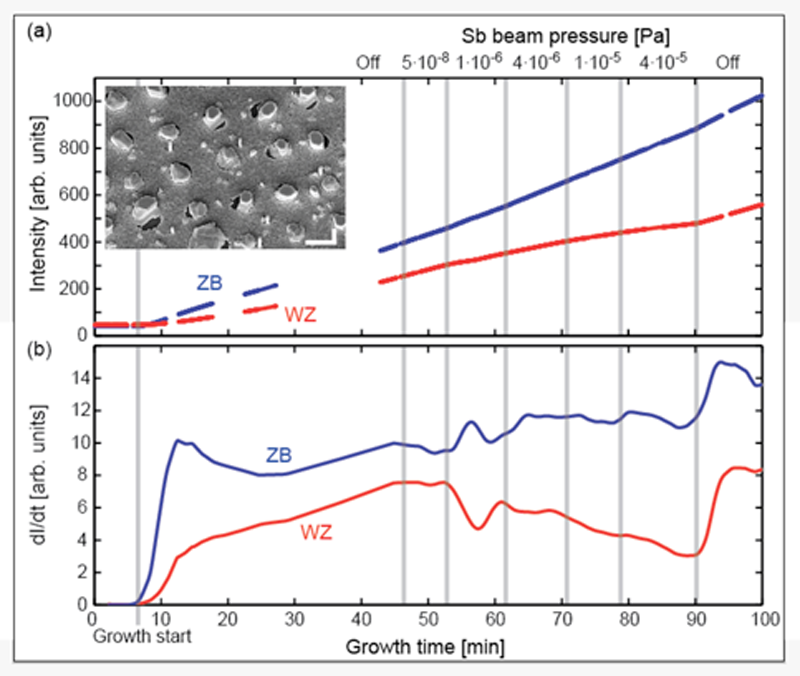
Fig. 1. Growth of InAs crystals on Si(111) under an increasing Sb pressure. a) The intensity of the [11-1]ZB and [10-11]WZ bragg peaks measured as a function of growth time. Inset shows a post growth scanning electron microscope image of the nanostructured array, which shows that the sample is covered with a rough layer of InAsSb. Scale bar is 1 μm. b) The time derivative of the intensity shown in a) showing a polytypic reconstruction from WZ to ZB and back again around 50-60 min into the growth, which takes place at a given Sb partial pressure. The growth rate has been linearly interpolated at growth times without measurements of the intensity.
Results and Discussion
For growth of patterned nanostructures of InAs we saw a direct effect of introducing Sb to the growth, as shown in the figure 1. For a very little Sb flux, the growth rate does not only seem to decrease slightly ingeneral, but there also appears to be a reconstruction from ZB to WZ and back again. It is noticeable that even a very little amount of Sb decreased the WZ formation rate and increased the ZB formation rate. As we measure on the tail of the ZB peak, the growth rates of ZB and WZ cannot be compared directly, but the relative formation rates can be compared. It has previously been reported that small amounts of Sb influences the growth of Au-assisted InAs nanowire (NW) growth [5]. Closing the Sb shutter at the end of the Sb deposition gives a surprising increase in the growth rate of the oriented nanostructures. We believe this is due to an increase in the surface mobility of the In adatoms.
In Fig.2 we show that it is not only the ZB and WZ polytypes, which are formed, but also the more exotic types 4H and 6H. According to Johansson et al. [4], this is a natural consequence of the probabilities of having random stacking which will lead to high order polytypes. The figure shows a reciprocal scan along L, where all polytypic periods in principle should be visible. The scan is acquired around 30-40 min into the growth, during a pure InAs growth period.
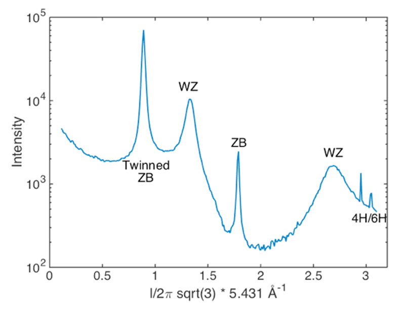
Fig. 2. Crystal truncation rod scan along the l direction obtained during growth of pure InAs. The scan is obtained in the time frame 30 min to 40 min of the growth shown in Fig.1, in which both the WZ and ZB growth rate is almost constant. The x-axis is plotted with respect to the Si substrate and thus all Bragg peaks are shifted with around 11% with respect to the InAs basis. The peak at l=3.05 is identified to be either the 4H or 6H crystal structure, as these two polytypisms are indistinguishable at this position. As in previous work [6], we have not identified the adjacent peak at l=2.9, which does not appear in the structure factor, but likely a result of higher order dynamical diffraction.
Challenges
The study combines several challenging experiments that all has to be optimized for a successful result. The MBE growth needs to be optimized for the specific substrates, such as preparation of oxide patterned silicon substrates, which needs pre-treatment before loading into the MBE system, where time and exposure to air is a critical parameter. It is also a further challenge that the X-ray beam should be aligned on a heated sample and that the samples degrade at elevated temperatures.
Conclusion
In conclusion, we have shown using an in-situ X-ray characterization setup that by using pre-patterned substrates for selected area growth of III-As nanostructures it is possible to measure polytypic phase formation dynamics, and follow the detailed evolution of the common structures ZB and WZ. This may lead to new insight into the mechanisms of III-V nanostructure growth, and exciting future experiments may be proposed on the basis of this study. Moreover, the effect of adding a small amount of Sb to the growth system was observed to have an immediate impact on the growth mechanisms, as it induced a solid phase polytypic reconstructions.
References
[1] G. Jacopin et al. J. Appl. Phys. 110, 064313 (2011).
[2] W. Zhou, X-J. Chen, J-B. Zhang, X-H. Li, Y-Q, Wang and A. F. Goncharov, Scientific Reports 4, 6472(2014).
[3] P. Krogstrup, M. H. Madsen et al. Appl. Phys. Lett. 100, 093103 (2012).
[4] J. Johansson et al. ACS Nano, 6 (7), 6142–6149 (2012).
[5] C. Thelander et al. Appl. Phys. Lett. 100, 232105 (2012).
[6] S. Mariager et al. Appl. Phys. Lett. 91, 083106 (2007).
ⒸJASRI
(Received: June 23, 2015; Early edition: October 26, 2015; Accepted: December 11, 2015; Published: January 25, 2016)