


Volume3 No.1
SPring-8 Section A: Scientific Research Report
Understanding Epitaxial Growth of Phase-Change Materials through Studies of the Local Structure
a Paul-Drude-Institut für Festkörperelektronik, Hausvogteiplatz 5-7, 10117 Berlin, Germany
b Nanoelectronics Research Institute, AIST, Tsukuba Central 4, Higashi 1-1-1 Tsukuba, Ibaraki 305-8562, Japan
- Abstract
-
Ge2Sb2Te5 (GST) thin films were grown epitaxially on (001)- and (111)-oriented substrates with control of the growth surface temperature obtained by in-situ quadrupole mass spectrometry (QMS). X-ray absorption near edge spectra (XANES) obtained on samples prepared on different substrate orientations and with different surface temperature were compared. The results show that the Ge2Sb2Te5 layers grown on (111) surfaces show a more pronounced rhombohedral distortion as compared to layers grown on (001)-oriented surfaces.
Keywords: GST, XANES, MBE
Background and Purpose
The need for faster, denser, and greener electronic storage driven by the constant expansion of the Internet and multimedia devices has led to the development of phase change memory (PCM). Unlike the well-known FLASH memory which suffers from serious scaling problems associated with memory storage viacharge, PCM uses differences arising from structural change for storage, specifically the resistivity differences between two phases. The phase-change compound GST is in many ways prototypical in that itexperiences dramatic changes in electronic properties between its melt-quenched amorphous and crystalline phases making it in many ways ideal for both optical and electrical storage applications. While the stable (bulk) crystalline phase of GST (bulk-GST) is a nine-layer rhombohedral structure, the phase used in devices is metastable (c-GST) and assumes a distorted rock salt structure. In devices, this phase is inevitably polycrystalline as it is grown from a melt-quenched amorphous phase. The small-grain polycrystalline nature of c-GST found in devices has lead to many questions regarding the details of the true nature of the crystalline phase as attempts to grow c-GST in bulk invariably lead to the formation of the rhombohedral phase. We have applied molecular beam epitaxy (MBE) to grow epitaxial films of c-GST using the substrate template mediated strain stabilization of the metastable phase.
Experimental Summary
In the MBE growth of c-GST, molecular sources of the constituent elements are provided using precisely temperature controlled effusion cells while a single crystal template substrate is heated to a carefully controlled temperature. For the case of GST growth, the constituent sources were elemental Ge, Sb, and Te and the substrates were InAs(001), InAs(111), Si(001) and Si(111). Experimentally it has been determined that epitaxial c-GST thin film growth occurs within a very narrow temperature range with amorphous film growth occurring for substrate temperatures Ts up to about 50°C, polycrystalline growth for 50°C< Ts<150°C, and crystalline growth for Ts up to 200°C [1]. The growth rate falls sharply for temperatures above 150°C reaching approximately zero for substrate temperatures of about 250°C. This narrow growth window for epitaxy is a cause for particular concern as changes in the emissivity of the substrate when it transforms from a bare Si wafer to a c-GST film lead to changes in radiative loss and changes in surface temperature even when the temperature of the substrate holder is precisely regulated. Another important question regards the kinetics of the desorption process and whether it leads to variations in composition as a function of depth. The desorbing flux has been investigated in-situ using QMS and the dominant desorption flux was found not to be elemental, but GeTe. As the GeTe desorption flux is strongly temperature activated, we have used this as a means to indirectly measure the surface temperature of the growing film. This signal is in turn used as a feedback parameter to control the surface temperature of the film. While the final film appears to be single crystalline, one area of critical concern remains whether there are compositional and/or structural variations within the (approximately 20 nm) thick film with thickness. To investigate this, we have grown a series of epitaxial c-GST films on Si(111) at different substrate temperatures with varying levels of GeTe desorption rates as measured by in-situ QMS. Each film grown on Si(111) and on Si(001) was capped by a 2 nm thick layer of amorphous ZnS-SiO2 alloy to inhibit oxidation due to air exposure. In contrast samples grown on InAs(001) and InAs(111) were uncapped. The epitaxial growth by molecular beam epitaxy (MBE) of GST on InAs(001) and InAs(111) is reported in Katmis et al. [1] while the one on Si(111) in Rodenbach et al. [2]. The growth by MBE of GeTe thin films on highly lattice-mismatched Si(111) substrates is reported in Giussani et al. [3].
Ge K-edge XANES measurements were done at BL01B1 in fluorescence mode at room temperature using a PILATUS detector in glancing exit geometry. In the experiment, the x-ray beam was directed at each sample at an incidence angle of three degrees, giving rise to an x-ray footprint on the sample of approximately 3 x 10 mm. A 100,000 element solid state detector (PILATUS) was setup orthogonally to the sample via a 1D Soller Slit cover to ensure that only fluorescence photons from the sample could reach the detector. The incident energy of the x-ray beam was then scanned through the Ge K-edge (11110 eV) over an approximately 1 keV range. The detecting elements of the PILATUS were configured in rows of approximately 200 (170 micron square) elements tall and approximately 500 (columns) elements along the x-ray axis. Each of the 200 rows were individually integrated along the column (x-ray) axis to yield 200 values for the integrated intensity each corresponding to a different exit angle for the fluorescence photons leaving the sample. The increased absorption of the x-ray fluorescence signal for small exit angles results in surface sensitive data as only photons emitted near the surface of the sample are able to reach the detector. The estimated best depth resolution is on the order of 1 nm. Each measurement was repeated twice and the obtained spectra were indistinguishable.
Results and Discussion
In Fig. 1, XANES spectra for GeTe grown on InAs(001) and InAs(111) are compared. One can see that while the overall features are very similar, the amplitude of the features is larger for the InAs(111) indicating a stronger short-range order, especially the feature at 11133 eV that is due to the presence of rhombohedral distortions [4].
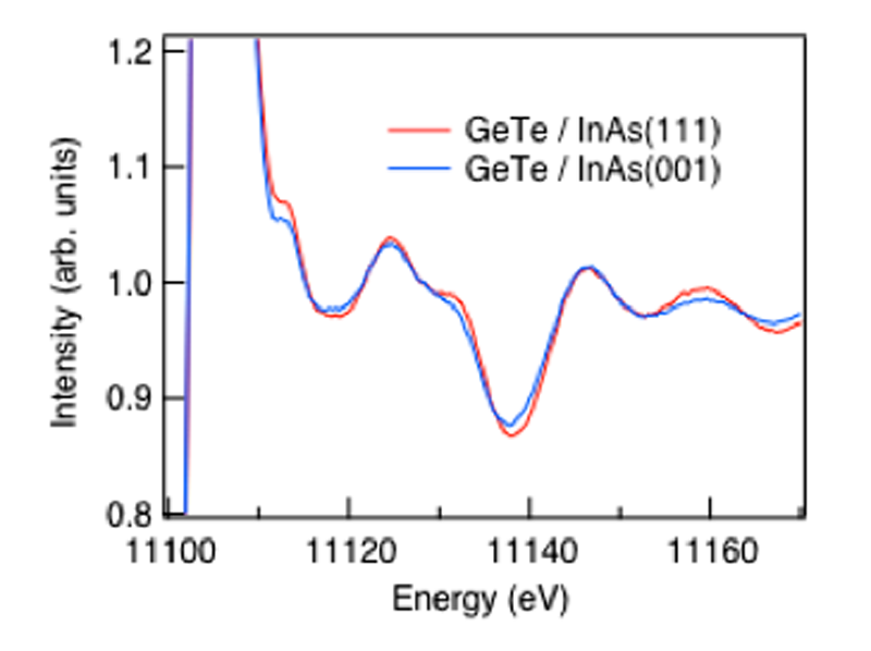
Fig. 1. XANES spectra for GeTe grown on InAs(001) and InAs(111)
The same trend was also observed for GST grown on InAs(001) and InAs(111) as shown in Fig. 2.
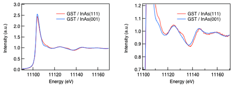
Fig. 2. XANES spectra for GST grown on InAs(001) and InAs(111)
In the zoomed image (Fig. 2 right) one can see that for the GST/InAs(001) the feature at 11133 eV is completely smeared out, while it is clearly observed for the case of the InAs(111) substrate. In addition, one can see that for the InAs(111) substrate the white line intensity is lower and a slope is less steep than for the InAs(001) case. A lower white line and the less steep slope suggest that the structure is locally more rhombohedrally distorted. The observed shift of the features at higher energies (11145 eV) indicating a shorter Ge-Te bond in the InAs(111) case is in agreement with the previous arguments [5].
Unexpectedly, we found that the layers grown on Si(001) substrates were oxidized despite otherwise identical growth conditions (Fig. 3), as is evidenced by an appearance of a strong feature around 11110 eV [6], characteristic of Ge-oxide. As AFM measurements (not shown) indicate the presence of a rough surface for growth on Si(001), suggesting that the oxidation may be a result of voids originating from the abutting of rhombohedrally distorted islands on the growth surface.
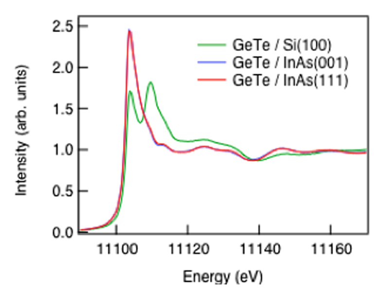
Fig. 3. XANES spectra for GeTe grown on InAs(001) and InAs(111) and on Si(001)
We have also studied the effect of the growth conditions (substrate temperature and GeTe desorption rate) on the sample structure of GST grown on Si(111). In this experiment, the samples were capped by ZnO-SiO2 to prevent oxidation. XANES data for two c-GST epitaxial samples for which 20% and 50% GeTe desorption rates were measured in-situ by QMS show that although the GeTe desorption rate more than doubled between the two films, no change in local structure about Ge atoms between the surface and bulk can be detected strongly suggesting that that the samples are uniform structurally along the growth direction. In a series of XANES scans for all films, a small feature near 11117 eV can be seen to appear in films with a slightly higher concentration of Ge corresponding to approximately a Ge2Sb1Te5 composition, while the remaining films have a Ge2Sb2Te5 composition. GeTe desorption rate was used to estimate the stoichiometry, using as a reference samples prepared with the same approach and measured by Rutherford backscattering. The depth dependent XANES signals for these two samples also confirms that the local structure about Ge atoms is the sample on the surface as the bulk, with both spectra indicating a slightly different bonding arrangement for Ge atoms. This bonding arrangement is currently being further investigated.
In conclusion, our results demonstrate that the film quality is higher for (111)-oriented samples and suggest that films grown on Si may be more easily oxidized.
Acknowledgements
We would like to acknowledge S. Behnke and C. Stemmler for technical support with the MBE. Synchrotron radiation was supplied by SPring-8. Partial support for this work was provided by the Deutsche Forschungsgemeinschaft (BR 1723/3-1) and the Japan Science and Technology Agency through an international research cooperation grant.
References
[1] F. Katmis, R. Calarco, K. Perumal, P. Rodenbach, A. Giussani, M. Hanke, A. Proessdorf, A. Trampert, F.Grosse, R. Shayduk, R. Campion, W. Braun and H. Riechert, Cryst. Growth Des. 11, 4606 (2011).
[2] P. Rodenbach, R. Calarco, K. Perumal, F. Katmis, M. Hanke, A. Proessdorf, W. Braun, A. Giussani, A.Trampert, H. Riechert, P. Fons and A. V. Kolobov, Phys. Status Solidi - Rapid Res. Lett. 6, 415 (2012).
[3] A. Giussani, K. Perumal, M. Hanke, P. Rodenbach, H. Riechert and R. Calarco, Phys. Status Solidi 249,1939 (2012).
[4] P. Fons, A. V Kolobov, M. Krbal, J. Tominaga, K. Andrikopoulos, S. Yannopoulos, G. Voyiatzis and T.Uruga, Phys. Rev. B 82, 2 (2010).
[5] A. V. Kolobov, P. Fons, A. I. Frenkel, A. L. Ankudinov, J. Tominaga and T. Uruga, Nat. Mater. 3, 703 (2004).
[6] L. Bertini, P. Ghigna, M. Scavini and F. Cargnoni, Phys. Chem. Chem. Phys. 5, 1451 (2003).
ⒸJASRI
(Received: April 28, 2014; Early edition: December 25, 2014; Accepted: January 16, 2015; Published: February 10, 2015)