


Volume7 No.2
SPring-8 Section A: Scientific Research Report
Effect of Film Thickness on Induction Time of Isothermal Crystallization from the Melt of Poly(3-hydroxybutyrate) Investigated by Time-resolved Grazing-incidence X-ray Scattering Measurements Using Synchrotron Radiation
aKyoto Institute of Technology, bRIKEN SPring-8 Center,
cJapan Synchrotron Radiation Research Institute, dTohoku University
- Abstract
-
Isothermal crystallization behaviors from the melt have been investigated for poly (3-hydroxybutyrate) (P3HB) thin films by time-resolved measurements of grazing-incidence X-ray scattering using synchrotron radiation. P3HB films with thicknesses of ca. 25 nm ~ 3.2 μm prepared on silicon substrates were cooled rapidly from the melt to a crystallization temperature, Tc, of 373 K by using a temperature-jump (T-jump) apparatus. Isothermal crystallization behaviors of P3HB in thin films were traced by simultaneous measurements of grazing-incidence wide-angle X-ray scattering (GIWAXS) and small-angle X-ray scattering (GISAXS). It was experimentally found for the first time that the induction time of crystallization became longer with reducing the film thickness. This indicated that the chain mobility necessary for nucleation at 373 K was reduced in thin films. It was also indicated that lamellar crystals having the edge-on type orientation to the substrate surface were preferentially formed at the beginning of crystallization. Those lamellae in the thin films might be stacked one another with amorphous chains in a disordered manner.
キーワード: crystallization kinetics, poly(3-hydroxybuthyrate) thin film, grazing-incidence small-angle and wide-angle X-ray scattering measurement using synchrotron radiation, induction time of crystallization, film-thickness effect
Background and Purpose
Polymer thin films are widely utilized as industrial materials such as organic solar cell, organic EL and FET. How to control crystallization behavior of polymers in thin films is one of important research topics in polymer science. Effect of film thickness on crystal growth and molecular mobility has been investigated by atomic force microscopy and dielectric spectroscopy[1-10]. It was reported that the linear growth rate of polymer crystals in the latter stage of crystallization decreased with reducing the film thickness. When local chain (segmental) mobility of polymers reduces, the glass transition temperature, Tg, of polymers increases. This results in decreasing the crystal growth rate of polymers in thin films. On the other hand, the segmental mobility of polymers is activated at the free surface where polymer chains have excess free volume. Therefore, the effective Tg in the surface region decreases. Since the surface-to-volume ratio of a film increases with reducing the film thickness, it is reasonable to consider that the crystal growth rate increases in thin films. Nevertheless, it was experimentally reported that the crystal growth rate decreased with reducing the film thickness. Is there no surface effect on crystallization kinetics for polymer thin films? In order to answer this question, film-thickness dependence of the primary nucleation rate of polymer crystals should be investigated on the molecular scale. In general, a plot of the primary nucleation rate of bulk polymers as a function of crystallization temperature, Tc, exhibits a bell-shape profile whose peak is observed almost at the middle temperature between the Tg and the melting point, Tm of polymers. As the Tg of polymers decreases with decreasing the film thickness, the peak temperature in the bell-shape plot might decrease[9]. It can be predicted that the primary nucleation rate of polymers in thin films might become lower at higher Tcs and higher at lower Tcs with decreasing film thickness. However, there is no experimental support for this prediction on the basis of film thickness effect as well as film surface effect.
The purpose of this study is to investigate the influence of film thickness on the induction time of crystallization and lamellar stacking of poly(3-hydroxybutyrate)(P3HB) in thin films in isothermal crystallization from the melt. The early-stage of crystallization behavior of linear polymers in thin films was traced on the molecular scale by time-resolved measurements of grazing-incidence wide-angle X-ray scattering (GIWAXS) and small-angle X-ray scattering (GISAXS) using synchrotron radiation.
Experimental Section
A sample used in this study was a commercially-available P3HB (Sigma-Aldrich Co., natural origin, R-chirality). The weight-average molecular weight, Mw, the number-average molecular weight, Mn, and the degree of polydispersity, Mw/ Mn, are 437k, 262k and 1.67, respectively. Crystal structure of P3HB reported by Yokouchi et al. is orthorhombic with the lattice constants a, b and c of 0.576 nm, 1.32 nm and 0.596 nm (the c axis is parallel to the chain axis)[11]. This crystal structure is called thea-form structure whose crystallographic space group is P212121. Two P3HB chains are packed in the α-form unit cell and each chain has 21 helical structure with a monomer conformation of (G2T2)2. A 0.1 wt% chloroform solution of P3HB was prepared at ca. 334 K under N2 atmosphere and then it was poured into methanol. As the precipitate was obtained as a purified P3HB, it was separated from the mixed solution of chloroform and methanol by decantation and filtration. The purified P3HB was dried at the ambient temperature. Thermal properties of the purified P3HB were evaluated at a heating rate of 10 K/min by the DSC2920X differential scanning calorimetry (TA Instruments, Inc.). Tg and Tm of the P3HB were 276 K and 444 K, respectively.
0.2, 2.0, 4.0 and 5.0 wt% chloroform solutions of the purified P3HB were prepared at 333 K under N2 atmosphere. Si substrates were cleaned by ultrasonic cleansing in the distilled water, methanol and acetone in order. The diameter and thickness of Si substrates were 7.5 mm and 0.5 mm, respectively. Crystallographic surface of the Si substrate was the cubic (100) plane and its top surface was covered with the native SiO2 layer. After a small amount of each solution was dropped onto the Si substrate surface at 293K, the substrate was rotated at a speed of 2000 rpm for 10 s. Film thickness was evaluated by the Nano Scope IIIa atomic force microscope (AFM) (Veeco Instruments Inc.) and/or Dektak Profilometer(Ulvac Inc.). Vertical resolutions in height measurements by AFM and Dektak were ca. 0.2 nm and 0.5 nm, respectively. The rectangular cantilever probe with a pyramidal tip was used for AFM observations. The probe was made of monolithicsilicon with a resonant frequency of ca. 320 kHz (Nano World Co.). The AFM observations were performed in the tapping mode under a constant load of 42 N/m at a scan rate of 20 μm/s. For Dektak profiling, a diamond probe was used and a scan rate was 125 μm/s. The thicknesses evaluated for spin-coated films with 0.2, 2.0, 4.0 and 5.0 wt% chloroform solutions were 25±5, 210±30, 390±60, and 3.2±0.6 µm, respectively.
Time-resolved simultaneous measurements of GIWAXS and GISAXS[12,13] were carried out to trace isothermal crystallization behaviors from the melt of P3HB in thin films. The X-ray refractive index of materials, n, is defined as n= 1 –δ+iβ. Here, δ= (λ2re/2π)N and β= (λ/4π)µ. re denotes the classical electron radius. N denotes the number of electrons per volume and is expressed as N= NAZρM-1 (NA: Avogadro's number, NA = 6.022×10²³ mol-1, Z: the atomic number, M: the atomic weight, ρ: density, μ: the linear absorption coefficient). The n of materials is less than 1.0 for X-rays. When a sample is irradiated by the incident X-rays at a grazing angle to the sample surface, αi, lower than the critical angle of total reflection of the sample, αc, total reflection of the incident X-rays occurs and only evanescent X-rays permeate the sample. The αc is expressed as αc = ![]() . When the wavelength of X-rays is 0.10 nm, the αcof the P3HB orthorhombic crystal is 0.109 and that of the Si crystal is 0.144 deg. The αiin this study was 0.11 deg., at which the direct X-rays penetrate the P3HB thin film and the total reflection of the direct X-rays occurred on the surface of a Si substrate. GIWAXS patterns were measured with a C9728DK-10 flat panel detector (FPD) (Hamamatsu photonics K. K., pixel resolution: 50×50 μm2). GISAXS patterns were detected with a combination of Image Intensifier (II) (Hamamatsu photonics K. K., pixel resolution: 106.4×106.4 μm2)and a C4742-98-24E charge coupled device (CCD) detector (Hamamatsu photonics K. K.). The sample-to-detector distances for GIWAXS and GISAXS measurements were 54.6 m and 2196 mm, respectively. A 2100 mm-length vacuum path was placed between the FPD and II+CCD detectors. Standard samples used to determine the sample-to-detector distances in GIWAXS and GISAXS measurements were silicon powder crystals and a dried chicken collagen fiber, respectively. The x, y, and z components of the scattering vector, q, in the rectangular coordinate system are defined as qx= (2π/λ)cos(αf)sin(2θf)cos(αi), qy= (2π/λ)sin(2θf)cos(αf), and qz= (2π/λ)(sin(αi) + sin(αf)). Here, the x and y coordinates were the horizontal axes, and the z coordinate was the vertical axis. The optical plane of the direct X-rays was the x-z plane. The 2θf and αf denote components of the take-off scattering angle in the x-y plane and along the z axis. Time-resolved measurements of GIWAXS and GISAXS using synchrotron radiation were carried out at the BL40B2 beamline. An irradiation time of X-rays per scattering pattern was 1-5 s and an interval time in the sequent measurements was 2-7 s.
. When the wavelength of X-rays is 0.10 nm, the αcof the P3HB orthorhombic crystal is 0.109 and that of the Si crystal is 0.144 deg. The αiin this study was 0.11 deg., at which the direct X-rays penetrate the P3HB thin film and the total reflection of the direct X-rays occurred on the surface of a Si substrate. GIWAXS patterns were measured with a C9728DK-10 flat panel detector (FPD) (Hamamatsu photonics K. K., pixel resolution: 50×50 μm2). GISAXS patterns were detected with a combination of Image Intensifier (II) (Hamamatsu photonics K. K., pixel resolution: 106.4×106.4 μm2)and a C4742-98-24E charge coupled device (CCD) detector (Hamamatsu photonics K. K.). The sample-to-detector distances for GIWAXS and GISAXS measurements were 54.6 m and 2196 mm, respectively. A 2100 mm-length vacuum path was placed between the FPD and II+CCD detectors. Standard samples used to determine the sample-to-detector distances in GIWAXS and GISAXS measurements were silicon powder crystals and a dried chicken collagen fiber, respectively. The x, y, and z components of the scattering vector, q, in the rectangular coordinate system are defined as qx= (2π/λ)cos(αf)sin(2θf)cos(αi), qy= (2π/λ)sin(2θf)cos(αf), and qz= (2π/λ)(sin(αi) + sin(αf)). Here, the x and y coordinates were the horizontal axes, and the z coordinate was the vertical axis. The optical plane of the direct X-rays was the x-z plane. The 2θf and αf denote components of the take-off scattering angle in the x-y plane and along the z axis. Time-resolved measurements of GIWAXS and GISAXS using synchrotron radiation were carried out at the BL40B2 beamline. An irradiation time of X-rays per scattering pattern was 1-5 s and an interval time in the sequent measurements was 2-7 s.
A T-jump apparatus was designed and assembled for this study. It consists of a sample stage with a diameter of 8 mm and two furnaces, the so-called high- and low-temperature ones. N2 gas was flown inside of the furnaces for preventing the sample from oxidization. A thin film on a Si substrate on a sample stage was melted at ca. 351 K for 5-10 min by using the high-temperature furnace. By exchanging the high-temperature furnace to the low-temperature furnace at the sample position (by T-jump), the thin film was rapidly cooled and kept at Tc. The isothermal crystallization time, t, was set to zero when the sample temperature reached Tc immediately after T-jump. The sample temperature was monitored with thermocouples attached to the film surface. A cooling rate of the sample was ca. 70 K / min in average. Temperature fluctuation of the sample after T-jump was ca. ± 0.4 K
Result and Discussion
Figures 1 shows GIWAXS patterns measured for P3HB thin films with thicknesses of 3.2±0.6 µm, 390±40 and 25±5 nm in isothermal crystallization processes at 373 K from the melt. At the beginning of GIWAXS measurements, isotropic scattering from the melt of P3HB was measured for all the films. As soon as the T-jump was completed, Debey-Scherrer rings were detected for the 3.2 µm-thick film as shown in Figure 1a. In the case of the 390 nm-thick film, Bragg reflections appeared as anisotropic peaks around t = ca. 74 s as shown in Figure 1b. As the strong anisotropic reflections and weak Debey-Scherrer rings were always detected, it was implied the primary nuclei generated having preferred crystallographic orientation. No reflection was able to be measured for the 25 nm-thick film by t = 1768 s as shown in Figure 1c. Figure 2 shows intensity profiles the GIWAXS patterns in Figure 1. The magnitude of intensity against q was obtained by calculating the azimuthal-angle averaged intensity per pixel in the GIWAXS pattern. All the observed peaks in Figures 1a and 1b were able to be indexed with the orthorhombic crystal lattice of P3HB. As time elapsed, these reflections increased in intensity. A footprint of the direct X-rays along the optical axis at the sample position was longer than the length of the film. Reflections from the film at different irradiated positions in the footprint were overlapped in GIWAXS patterns. As a result, reflections were observed as broad peaks. From the position of double peaks indexed as the 020 reflection, difference in camera length was estimated. It was found that the magnitude of the camera-length difference between these peaks was almost consistent with the length of the substrate along the optical axis. Therefore, it was considered that the 020 reflection from the slightly-thicker area of the film at the near- and far-edges of the substrate to the detector were observed partly-separated broad peaks as shown in Figure 2b. When the <020> direction is parallel to the crystallographic b axis, the crystallographic c axis is parallel to the qxy plane. Therefore, the P3HB chains in the crystal state had a strong tendency to orient parallel to the substrate surface. This means that the edge-on nuclei mainly generated and grew in the 390 nm-thick film of P3HB. Figure 3 shows intensity change of the 020 reflection as a function of t for the P3HB thin films with thicknesses of ca. 25, 210, 390 nm and 3.2 µm. The time period until the 020 reflection appeared and started to increase in intensity after completion of T-jump (t = 0 s) was evaluated in Figure 3 as the so-called induction time of crystallization, tcrystal. The tcrystal evaluated for the films with thicknesses of ca. 210, 390 nm and 3.2 µm was 186, 18 and 4 s, respectively, as indicated with arrows. As the 020 reflection didn’t appear for the films with thicknesses of ca. 25 nm, the tcrystal was unable to be determined in this study.
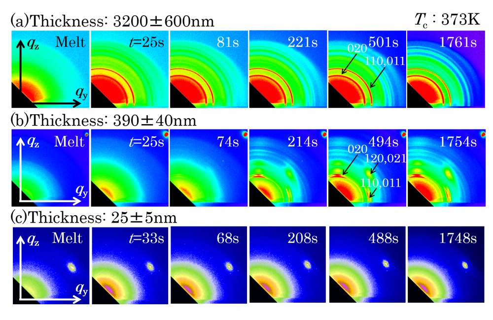
Figure 1. GIWAXS patterns measured for P3HB thin films with thicknesses of 3.2 ± 0.60 µm (a), 390 ± 40 nm (b) and 25 ± 5 nm (c) in isothermal crystallization processes at Tc = 373 K.

Figure 2. Intensity profiles of GIWAXS patterns in Figure 1. Thicknesses of the P3HB films were 3.2 ± 0.60 µm (a), 390 ± 40 nm (b) and 25 ± 5 nm (c).
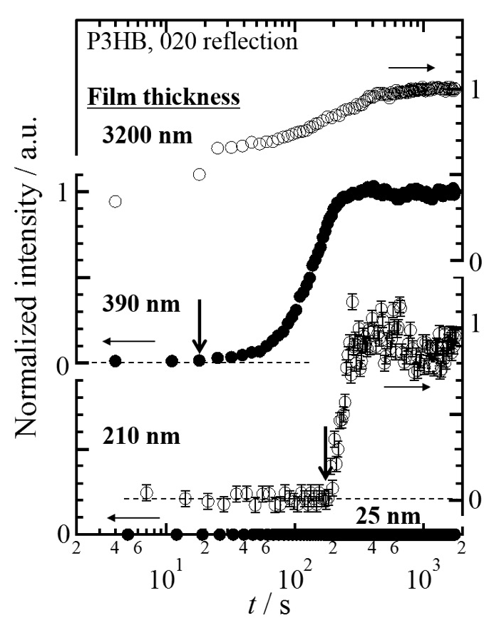
Figure 3. Intensity change of the 020 reflection of the P3HB orthorhombic crystal as a function of isothermal crystallization time, t, measured for the P3HB thin films with thicknesses of ca. 3.2 µm, 390 nm, 210 nm and 25 nm.
Figure 4 shows in-plane and out-of-plane intensity profiles of the GISAXS patterns measured for the P3HB thin films with thicknesses of ca. 3.2 µm (a), 390 nm (b) and 25 nm (c). The lamellar stacking distance (long period), L, was estimated from the peak position of the primary peak. The magnitudes of L in the in-plane and out-of-plane directions were ca.7.5 and 7.2 nm for the 3.2 µm-thick film, respectively. The magnitudes of L in the out-of-plane direction was ca. 7.5 nm for the 390 nm-thick film. There was no peak in the in-plane profiles measured for the 390 nm-thick film in Figure 4b. This indicated that formed lamellae were isolated or stacked one another in a disorder manner as shown in Figure 5. No peak was observed in the in-plane and out-of-plane profiles for the 25 nm-thick film in Figure 4c because crystallization didn’t occur. The time period until the primary peak appeared and started to increase in intensity after completion of T-jump (t = 0 s) was evaluated as the induction time of formation of lamellar stacking structure, tlamellae. The tlamellae evaluated for the P3HB thin films with thicknesses of ca. 390 nm and 3.2 µm were 60 and 4 s, respectively. Figure 6 shows film thickness dependencies of the tcrystal and tlamellae. It was experimentally found that tcrystal became longer with reducing the thickness of P3HB films. This indicates that the primary nucleation rate of P3HB crystals decreased with reducing the film thickness. Segmental mobility of polymer chains may be reduced in the internal part of thin films whose spatial dimensions are apparently reduced. It was reasonable to consider that transportation and alignment of P3HB segments having the order conformation for crystallization might become slower with reducing the film thickness. Here, the number of ordered chain conformation depended on the Boltzmann statistics. Another reason why the primary nucleation rate of P3HB crystals decreased with reducing the film thickness might relate to the surface effect. The primary nucleation rate for polymers against Tc is explained with a bell-shape curve having a peak around the middle temperature between Tg and Tm. For P3HB in the bulk, the middle temperature between Tg and Tm was ca. 360 K. The Tc of 373 K in this study was higher than 360 K. If Tg of thin films would decrease with reducing the film thickness due to higher molecular mobility of chains in the film surface, the middle temperature between lower Tg and Tm would shift to the lower temperature[9]. This suggests that the primary nucleation rate for P3HB at the Tc of 373 K would also decrease with reducing the film thickness. This expectation on correlation between film thickness and the primary nucleation rate was consistent with experimental results in this study. There was a possibility that the chain-confinement effect in the internal part of the film and/or the surface effect on activated segmental mobility of P3HB became evident in terms of the primary nucleation rate. The tlamellae became longer with reducing the film thickness. Also, the tlamellae evaluated for each film thickness was longer than the tcrystal. As lamellar stacking occurred after isolated lamella was generated, it was considered that the tlamellae in the thin films also depended on the diffusion-limited molecular mobility.
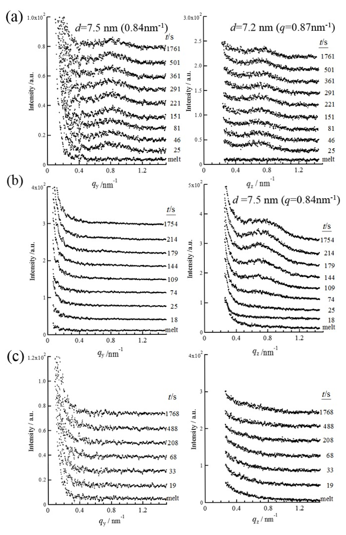
Figure 4. In-plane (left) and out-of plane (right, at qy=0.44 nm-1) intensity profiles of GISAXS patterns measured for P3HB thin films during crystallization at 373 K from the melt. Thicknesses of the films were 3.2 ± 0.60 m (a), 390 ± 40 nm (b) and 25 ± 5 nm (c).
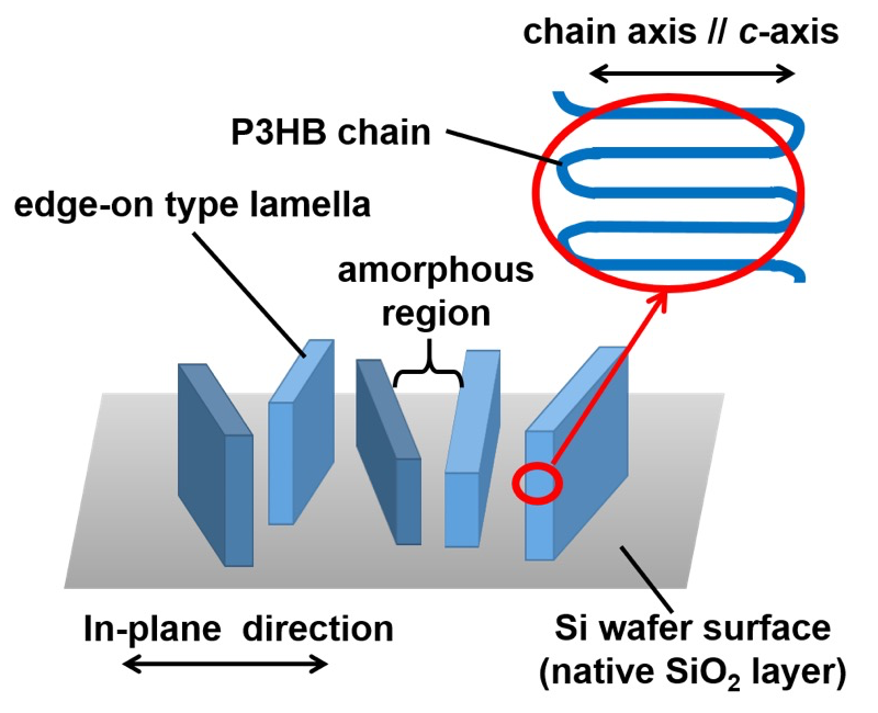
Figure 5. Schematic explanation of disordered stacking of the edge-on type P3HB lamellae in the in-plane direction.
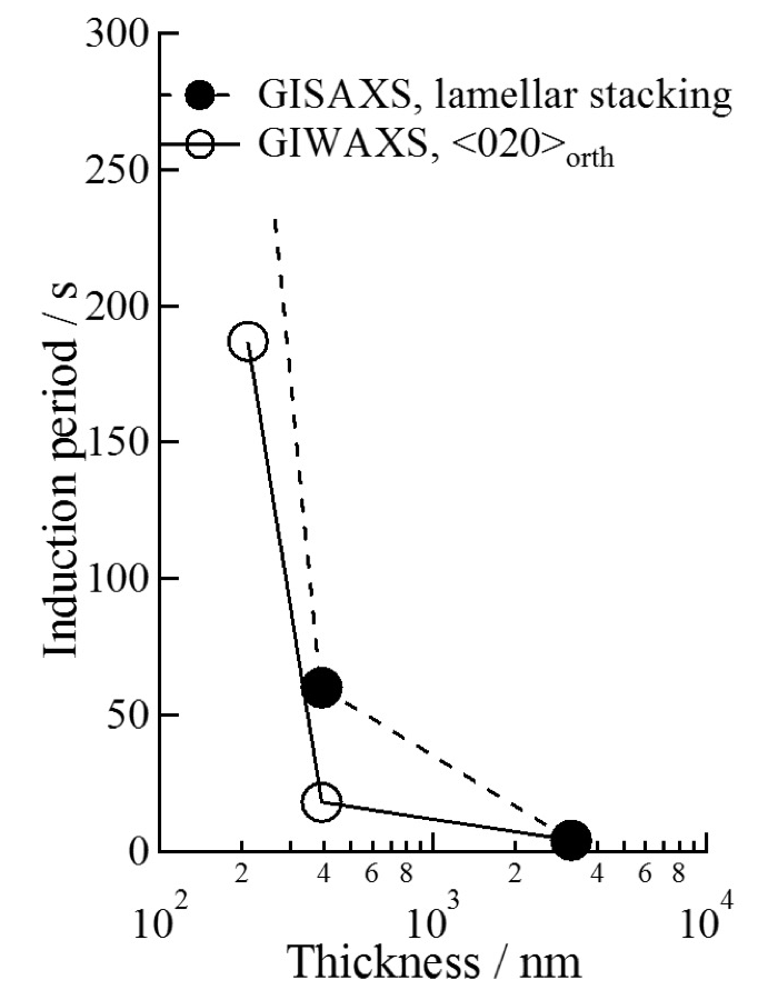
Figure 6. Film thickness dependences of the induction time of crystallization (○) evaluated from GIWAXS profiles and lamellar stacking (●) evaluated from GISAXS profiles.
Acknowledgment
This work was partly supported by Grant-in-Aid for Scientific Research on Innovative Areas (No.2107) of Japan Society for the Promotion of Science (JSPS). The synchrotron radiation experiments were performed at BL40B2 in the SPring-8 with the approval of the Japan Synchrotron Radiation Research Institute (JASRI) (Proposal No. 2010B1433, 2011A1446 and 2011B1464).
Reference
[1] S. Sawamura et al., J. Phys. Soc. Jpn., 67, 3338-3341 (1998).
[2] K. Taguchi et al., Polymer, 42, 7443-7447 (2001).
[3] K. Taguchi et al., J. Macromol. Sci. B, 45, 1033-1042 (2002).
[4] K. Taguchi, A. Toda and Y. Miyamoto, J. Macromol. Sci. B, 45, 1141-1147 (2006).
[5] S. Napolitano and M. Wubbenhorst, J. Phys. Conds. Matter, 19, 205121 (2007).
[6] S. Napolitano and M. Wubbenhorst, J. Phys. Chem. B, 111, 5775-5780 (2007).
[7] S. Napolitano and M. Wubbenhorst, Macromolecules, 39, 5967-5970 (2006).
[8] M. J. Capitan, D. R. Rueda and T. A. Ezquerra, Macromolecules, 37, 5653-5659 (2004).
[9] Yong Wang et al., Macromolecules, 41, 2548-2553 (2008).
[10] Katsuhito Mori et al., Macromolecules, 41, 1713-1719 (2008).
[11] M. Yokouchi et al., Polymer, 14, 267-272 (1973).
[12] S. Sasaki et al., J. Appl. Cryst., 40, s642-s644 (2007).
[13] S. Sasaki et al., J. Phys. Conf. Seri., 184, 012015 (2009).

(Received: April 8, 2019; Early edition: July 8, 2019; Accepted: July 16, 2019; Published: August 29, 2019)