


Volume7 No.1
SPring-8 Section A: Scientific Research Report
Electronic Properties of Doped Topological Insulators (BiMn)2Te3 by means of Bulk Sensitive Hard X-ray Photoemission
aCNR-IOM, bNIMS
- Abstract
-
The influence of magnetic dopants on the electronic structures of topological insulators (TIs) is a key factor for magnetic TIs-based spintronic application. Here we measured core level and valence band hard x-ray photoemission (HAXPES) spectra for (BiMn)2Te3 single crystals as a function of Mn doping to investigate the modification of the bulk band structures of Bi2Te3 by the dopants.
Keywords: Topological insulators, Magnetic dopants, HAXPES
Background and Purpose
Topological insulators (TIs) have attracted much attention in recent years due to their peculiar surface states which are spin-polarized and having a Dirac cone in the bulk band gap [1]. The surface states are the consequence of the bulk band inversion due to the strong spin-orbit interaction. The exceptional properties of the surface states make them be promising materials for future devices [2]. Recently ferromagnetic order was found in Mn doped TI Bi2-xMnxTe3[3]. Since then intense researches have been performed both theoretically and experimentally [4-9]. Although Mn dopants at the substitutional position of Bi should act as acceptors, numbers of experimental researches show electron-like conductivity [10]. The formation of ferromagnetic order in TIs is of interest for building topological insulator-based spintronics devices [11]. However, the mechanism of the magnetic long-range order as well as detailed electronic structure of the Mn doped TI are still unclear. Since TIs are characterized by their surface states, most experimental researches on TIs were dedicated to the measurements of the surface electronic structures. The properties of the materials are, however, determined by the bulk electronic structures. In this sense bulk sensitive HAXPES is an ideal tool to investigate electronic structures of Mn doped TIs. Comparison of valence band HAXPES in pure Bi2Te3 and magnetically doped (BiMn)2Te3 will reveal what are the relevant states modified by the magnetic dopants and where is located the Mn contribution.
Experimental Summary
HAXPES experiments were performed for single crystals Bi2-xMnxTe3 at BL15XU. We have prepared 4 samples with x = 0.10, 0.07, 0.04, and 0 in order to observe systematic changes of spectral features as a function of Mn concentration. High resolution HAXPES spectra were measured with hν = 6 keV at room temperature for Bi and Te core levels, and valence bands. Normal emission set up (take off angle 88°) was chosen in order to maximize the bulk sensitivity. The total resolution was set to be 150 meV. The Fermi energy (EF) and the binding energy (EB) of the spectra were calibrated by the valence band spectra for a Au reference sample.
Results and Discussion
Figure 1 shows the comparison of the valence band HAXPES spectra for Bi2Te3 (black) and Bi1.9Mn0.1Te3 (blue). The clear shift in energy of the Bi1.9Mn0.1Te3 valence band spectrum is observed toward higher binding energy side compared to Bi2Te3 valence band spectrum by approximately 80 meV. This shift is considered due to the occupation of the states created in the band gap above the top of the valence band of Bi2Te3 by Mn doping. Then EF of Bi1.9Mn0.1Te3 is pinned on the Mn induced states. This is seen better when we shift the Bi2Te3 valence band spectrum (Figs.2 (b) and (c)). The amount of shift was determined by the energy shift of Te 4d core levels of Bi2Te3 and Bi1.9Mn0.1Te3. The energy shift of Te 4d was obtained by the fitting with Voigt function and Shirley step function shown in Fig.2 (a). The intensity was normalized so as to minimize the sum of the square of the difference between two spectra for the binding energy range between 6.0 and 7.5 eV. Zoom up of the spectra close to EF is shown in Fig.2 (c). The light blue shaded area shows the contribution from the Mn induced state on the Bi1.9Mn0.1Te3 HAXPES spectrum.
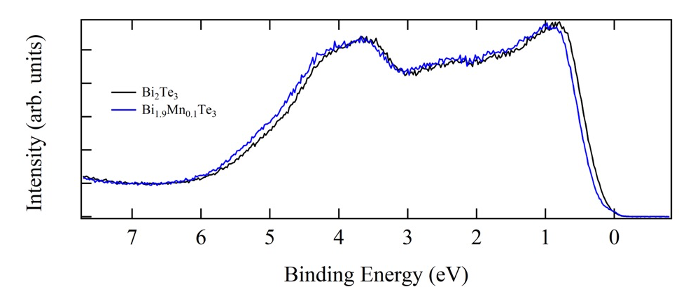
Fig. 1. Valence band HAXPES spectra for Bi2Te3 (black) and Bi1.9Mn0.1Te3 (blue). The clear shift in energy of the Bi1.9Mn0.1Te3 valence band spectrum is observed.
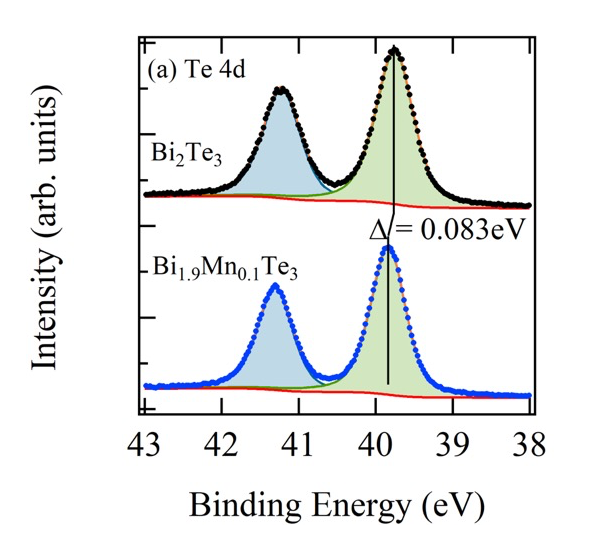
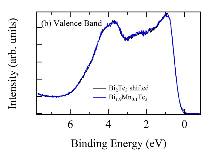
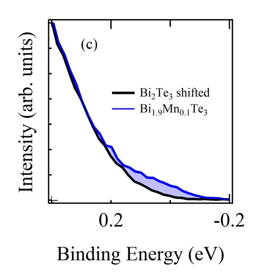
Fig. 2. (a) The shift of the Te 4d peaks obtained by the fitting. The black (Bi2Te3) and blue (Bi1.9Mn0.1Te3) dots denote the measured spectra. (b) Comparison of two valence band HAXPES spectra after the shift of Bi2Te3 valence band spectrum. (c) Zoom up around EF. The increase of the intensity at EF due to the Mn doping is clearly observed.
Bulk Bi2Te3 is a semiconductor with the band gap of 150 meV [12]. As observed in low energy angle-resolved PES spectra, surface band bending is commonly induced on Bi2Te3 by defects at the surface. Mn dopants modify the number of electrons in the surface states, which modifies the surface band bending, resulting in the energy shift of bulk band structure in the photoemission spectra [4]. It should be noted, however, that the carrier density of Bi1.9Mn0.1Te3 is quite high (> 7 x 1019 cm-3) and the band bending region is less than 10 nm from the surface. On the other hand the probing depth of HAXPES for nearly 6keV kinetic energy is about 20 nm, which is much larger than the surface band bending region. And the surface state contribution to the spectra is quite small. These mean that even though the band bending remains at the surface of Bi1.9Mn0.1Te3, the measured spectrum reflects well the real “bulk” band structure. Suppose that the doped Mn atoms simply add electrons to the bulk system, which results in the filling of the conduction band of Bi2Te3. The Fermi level will be in the conduction band of Bi2Te3, which is 150 meV above the valence band top. Eventually it should make a larger shift of the band than what is actually observed by the measurements. In order to clarify the modification of the valence band by Mn doping, we made the subtraction of the Bi2Te3 valence band spectra from Bi2-xMnxTe3 which are shifted in energy with the same manner as Fig.2. The shift for Bi1.96Mn0.04Te3 and Bi1.93Mn0.07Te3 are 0.004 and 0.013 eV, respectively. The difference spectrum for x =0.04 (green), 0.07 (red) and 0.10 (blue) are shown in Fig.3 with the Bi2Te3 valence band spectrum (black), which is multiplied by 1/4. From the blue spectrum of Fig. 3, one can clearly observe the Mn doped related peak at EF. The spectra for the doping of x = 0.04 and 0.07 do not show such a peak but the decrease of the intensity at EF. The absence of the Mn induced peak at EF for x = 0.04 and 0.07 can be attributed to their relatively low carrier densities. They are 3.5 x 10¹⁸ and 5 x 1018 cm-3 for x = 0.04 and 0.07, respectively, which are more than one order of magnitude smaller than that of x = 0.10. In fact the shifts of spectra for x = 0.04 and 0.07 are much smaller than that for x = 0.10. Except for this all of three spectra have the same tendency between EB = 1 eV and EF. Another Mn doping effect is observed between EB = 1.5 and EB = 3 eV. It is the contribution of Mn 3d states according to calculations [5,9]. Since the top of the valence band of Bi2Te3 (the peaks at EB = 1 eV) is mainly the contribution from Te 5p states [9], the observed features of the difference spectra imply the modification of the Te 5p density of states by Mn doping.
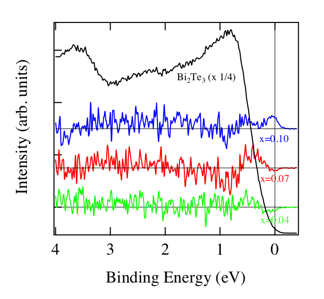
Fig.3. Summary of the difference spectra for three doping concentration. Note that the difference spectra are offset for clarity. Black horizontal lines are the zero lines for each difference spectrum.
Challenges
We measured also angle-resolved HAXPES spectra for the TIs with hν = 3 keV at low temperature (T = 25 K) in the proposed beamtime. We did not, however, observe any band dispersion in the spectra, which can be attributed to the rather low Debye temperature (Bi2Te3, 165 K) of the system [13]. Recently developed soft x-ray angle-resolved PES experiments may be an alternative tool for revealing the momentum-resolved density of states of the bulk region in this system [14].
References
[1] M. Z. Hasan, C. L. Kane, Rev. Mod. Phys. 82, 3045 (2010).
[2] X.-L. Qi and S.-C. Zhang, Phys. Today 63, 33 (2010).
[3] Y. S. Hor et al., Phys. Rev. B 81, 195203 (2010).
[4] I. Vobornik et al., J. Phys. Chem. C 118, 12333 (2014).
[5] C. W. Niu et al., Appl. Phys. Lett. 98, 252502 (2011).
[6] A. Ghasemi et al., APL Materials 4, 126103 (2016).
[7] J. Růžička et al., New J. Phys. 17, 013028 (2015).
[8] K. Carva et al., Phys. Rev. B 93, 214409 (2016).
[9] V. N. Antonov et al., Phys. Rev. B 96, 224434 (2017).
[10] R. Tarasenko et al., Physica B, 481, 262 (2016).
[11] L. He, X. Kou, and K. L. Wang, Phys. Status Solidi RRL 7, 50 (2013).
[12] G. A. Thomas et al., Phys. Rev. B 46, 1553 (1992).
[13] C. S. Fadley, J. Electron Spectrosc. Relat. Phenom. 190, 165 (2013).
[14] V. N. Strocov et al., J. Synchrotron Radiat. 21, 32 (2014).
ⒸJASRI
(Received: March 30, 2018; Early edition: October 30, 2018; Accepted: December 17, 2018; Published: January 25, 2019)